
Light-emitting diode element and light-emitting diode device

A technology for light-emitting diodes and components, applied in electrical components, electric solid-state devices, semiconductor devices, etc., can solve the problems of insufficient luminous intensity, uneven current density, uneven luminous distribution, etc., and achieve luminous efficiency and internal quantum efficiency. The effect of reducing inhibition, easy heat dissipation, and alleviation of concentration

Inactive Publication Date: 2012-11-21
PANASONIC CORP
View PDF10 Cites 9 Cited by
  • Summary
  • Abstract
  • Description
  • Claims
  • Application Information

AI Technical Summary

Problems solved by technology

Therefore, the part with high current density generates heat, causing a problem that the luminous efficiency decreases.
Moreover, due to the resistance of the n-type conductive layer 102, it is not easy to apply a bias (bias) to the region of the active layer 103 away from the n-type surface electrode 106, and sufficient current cannot flow.
Therefore, sufficient luminous intensity cannot be obtained
Moreover, due to the uneven current density, the luminous distribution is also uneven
[0026] In this way, although the double-sided electrode type has a uniform current density and a structure that is easy to input high power, there is a problem that the reliability of mounting is low.
On the other hand, the surface electrode type is mounted using bumps, so it has high reliability, but there are problems of uneven current density and low efficiency when inputting large power

Method used


Image

  • Light-emitting diode element and light-emitting diode device
  • Light-emitting diode element and light-emitting diode device
  • Light-emitting diode element and light-emitting diode device

Examples


Embodiment approach 1

[0120] Figure 8 (a) is a cross-sectional view showing the light emitting diode device 31A of the first embodiment. Figure 8 (b) means Figure 8 (a) is a plan view of the back surface of the light emitting diode element 30A shown. Figure 8 (c) is a plan view showing the main surface of the light emitting diode element 30A. in addition, Figure 8 (a) is along Figure 8 (c) Cross-sectional view of line A-A'. exist Figure 8 (a) ~ (c) pair and Figure 6 (a) to (c) The same components are denoted by the same reference numerals.

[0121] Such as Figure 8 As shown in (a), a light emitting diode device 31A of this embodiment has a structure in which a light emitting diode element (chip) 30A is mounted on a mounting substrate 12 via bumps 10 and 11 . The light emitting diode element 30A is mounted on the mounting substrate 12 with its principal surface facing downward. The bump 10 connects the p-type electrode 5 of the light emitting diode element 30A and the mounting sub...

Embodiment approach 2

[0151] Figure 10 (a) is a cross-sectional view showing the light emitting diode device 31B of the second embodiment. Figure 10 (b) means Figure 10 (a) is a plan view of the back surface of the light emitting diode element 30B shown. Figure 10 (c) is a plan view showing the main surface of the light emitting diode element 30B. in addition, Figure 10 (a) is along Figure 10 (c) Cross-sectional view of line A-A'. exist Figure 10 (a) ~ (c) pair and Figure 8 (a) to (c) The same components are denoted by the same reference numerals.

[0152] Such as Figure 10 As shown in (a), in the light emitting diode device 31B of this embodiment, the second region 2b (the part of the n-type conductive layer 2 located around the through hole 8) in the main surface 2d of the n-type conductive layer 2 is provided with There is an insulating film 16 . On the second region 2 b of the main surface 2 d of the n-type conductive layer 2 , the n-type surface electrode 6 is arranged via a...

Embodiment approach 3

[0158] Figure 11 (a) is a cross-sectional view showing a light emitting diode device 31C according to the third embodiment. Figure 11 (b) means Figure 11 (a) is a plan view of the back surface of the light emitting diode element 30C shown. Figure 11 (c) is a plan view showing the main surface of the light emitting diode element 30C. in addition, Figure 11 (a) is along Figure 11 (c) Cross-sectional view of line A-A'. exist Figure 11 (a) ~ (c) pair and Figure 10 (a) to (c) The same components are denoted by the same reference numerals.

[0159] Such as Figure 11 As shown in (a), in this embodiment, no concave portion 20 is provided (in Figure 10 (a) et al.). The via hole 8 not only penetrates the n-type conductive layer 2 , but also penetrates the active layer 3 and the p-type conductive layer 4 .

[0160] The insulating film 15 is provided on the inner walls of the n-type conductive layer 2 , the active layer 3 , and the p-type conductive layer 4 constituti...


PUM


Abstract

A light-emitting diode element comprising: an n-type conductive layer (2) which comprises a first region (2a), a second region (2b) and a back surface (2c); an active layer (3) and a p-type conductive layer (4) both of which are arranged on the first region (2a) of the n-type conductive layer (2); a p-type electrode (5) which is arranged on the main surface of the p-type conductive layer (4); an insulating film (15) which is arranged on the inner wall of a through-hole (8) that penetrates through the n-type conductive layer (2) and has an opening on the second region (2b) and the back surface (2c) of the n-type conductive layer (2); a conductive part (9) which is arranged on the surface of the insulating film (15) in the inside of the through-hole (8); an n-type surface electrode (6) which is arranged in the second region (2b) and is in contact with the conductive part (9); and an n-type back-side electrode (7) which is arranged on the back surface (2c) of the n-type conductive layer (2) and is in contact with the conductive part (9).

Description

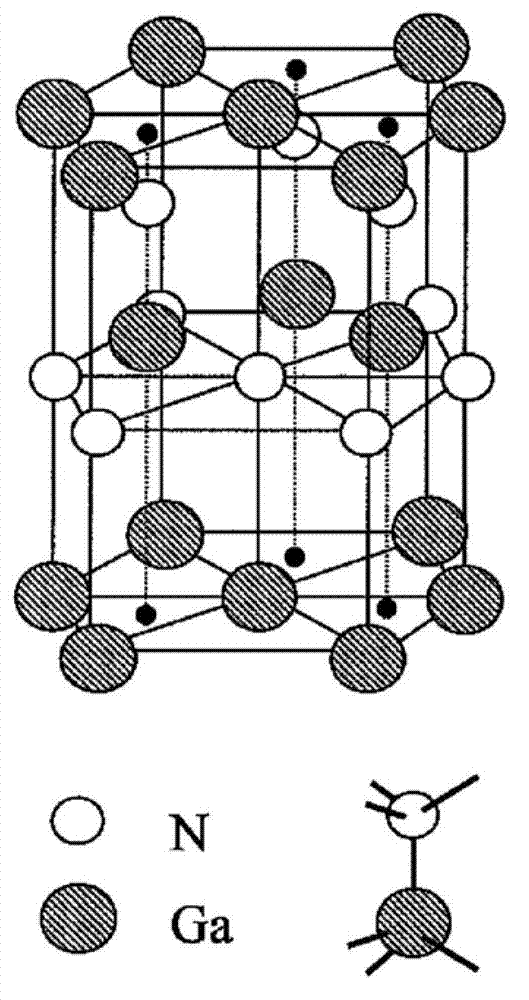
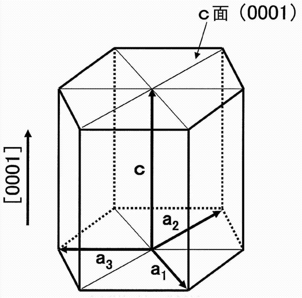
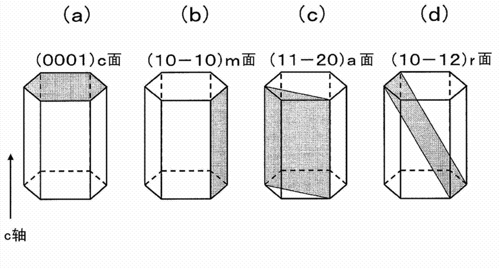
technical field [0001] The invention relates to a light-emitting diode element and a light-emitting diode device, in particular to a light-emitting diode element and a light-emitting diode device with through holes. Background technique [0002] Nitride semiconductors having nitrogen (N), which is a group V element, are expected to be used as materials for short-wavelength light-emitting elements due to their large band gaps. Among them, research on gallium nitride-based compound semiconductors (GaN-based semiconductors) is being extensively carried out, and blue light-emitting diodes (LEDs), green LEDs, and semiconductor lasers made of GaN-based semiconductors have also been practically used (for example, refer to patent documents 1, 2). [0003] GaN-based semiconductors have a wurtzite crystal structure. figure 1 A unit cell of GaN is schematically shown. in Al a Ga b In c In N (0≦a, b, c≦1, a+b+c=1) semiconductor crystals, figure 1 A part of Ga shown can be replace...

Claims


Application Information

Patent Timeline
Patent Type & Authority Applications(China)
IPC IPC(8): H01L33/36H01L33/32
CPCH01L2933/0016H01L33/62H01L2224/73265H01L33/382H01L2224/48091H01L2924/00014
Inventor 岩永顺子横川俊哉山田笃志
Owner PANASONIC CORP
Learn More