Semiconductor linear galvanostat

A linear constant current, semiconductor technology, applied in the direction of semiconductor devices, electric solid state devices, lighting devices, etc., can solve the problems of high cost and complex structure, and achieve the effect of simple structure

Inactive Publication Date: 2012-11-28
UNIV OF ELECTRONICS SCI & TECH OF CHINA
View PDF4 Cites 0 Cited by
  • Summary
  • Abstract
  • Description
  • Claims
  • Application Information

AI Technical Summary

Problems solved by technology

However, it also has the disadvant...

Method used


Image

  • Semiconductor linear galvanostat
  • Semiconductor linear galvanostat
  • Semiconductor linear galvanostat

Examples


Embodiment 1

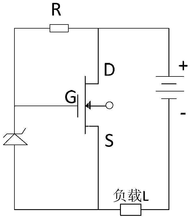
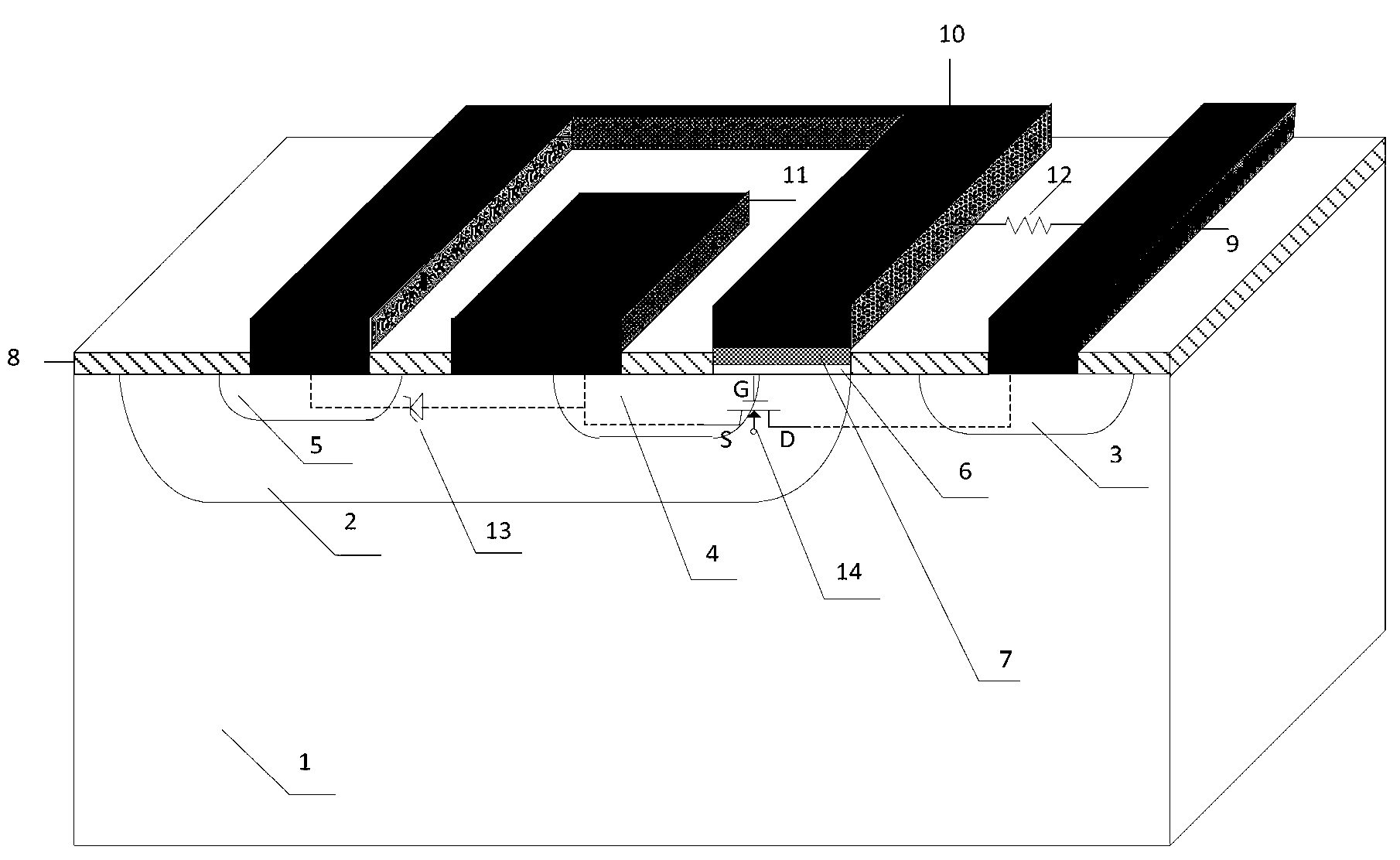
[0018] A semiconductor linear constant current device, such as image 3 As shown, it includes an N-type substrate 1, a P-type well region 2, a first N+ region 3, a second N+ region 4, and a third N+ region 5; wherein the P-type well region 2 and the first N+ region 3 are located on the N-type substrate bottom 1 top, and the P-type well region 2 and the first N+ region 3 are isolated from each other; the second N+ region 4 and the third N+ region 5 are located in the P-type well region 2 and are isolated from each other; the second N+ region 4 is located in the first N+ Between the region 3 and the third N+ region 5; the surface of the first N+ region 3 is connected to the first metal electrode 9; part of the second N+ region 4 and the P-type well region between the first N+ region 3 and the second N+ region 4 The surface of the gate oxide layer 2 has a gate oxide layer 6, the surface of the gate oxide layer 6 is a polysilicon gate electrode 7, and the surface of the polysilicon...

Embodiment 2

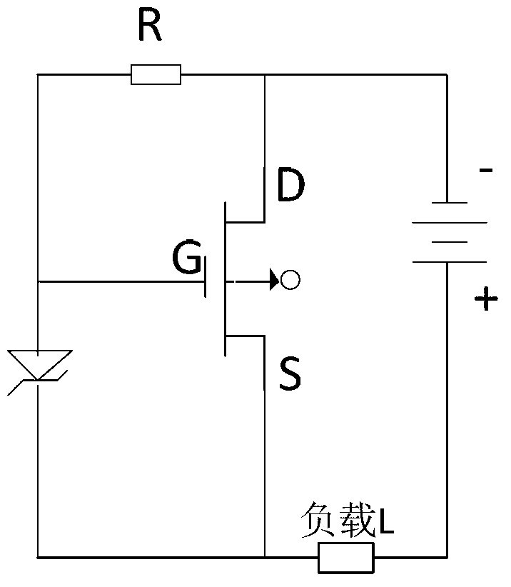
[0020] A semiconductor linear constant current device, such as image 3 As shown, it includes a P-type substrate 1, an N-type well region 2, a first P+ region 3, a second P+ region 4, and a third P+ region 5; wherein the N-type well region 2 and the first P+ region 3 are located on the P-type substrate bottom 1 top, and the N-type well region 2 and the first P+ region 3 are isolated from each other; the second P+ region 4 and the third P+ region 5 are located in the N-type well region 2 and are isolated from each other; the second P+ region 4 is located in the first P+ Between the region 3 and the third P+ region 5; the surface of the first P+ region 3 is connected to the first metal electrode 9; part of the second P+ region 4 and the N-type well region between the first P+ region 3 and the second P+ region 4 The surface of the gate oxide layer 2 has a gate oxide layer 6, the surface of the gate oxide layer 6 is a polysilicon gate electrode 7, and the surface of the polysilicon...


PUM


Abstract

The invention discloses a semiconductor galvanostat which belongs to the technical field of semiconductor devices. The semiconductor galvanostat comprises an MOSFET (Metal Oxide Semiconductor Field Effect Transistor) (14), a voltage stabilizing diode (13) and a current limiting resistor (12) which are integrated on the same chip. One end of the voltage stabilizing diode is connected with the grid G of the MOSFET, the other end of the voltage stabilizing diode is connected with the source S of the MOSFET, one end of the current limiting resistor is connected with the drain D of the MOSFET, and the other end of the current limiting resistor is connected with the grid G of the MOSFET. The voltage stabilizing diode can be used for clamping a voltage of the grid of the MOSFET, so that the current ID of a drain source of the MOSFET is maintained constant; and the current limiting resistor R can inhibit the current of the voltage stabilizing diode. The current limiting resistor can be a polycrystalline silicon resistor and also be a trap resistor. The semiconductor galvanostat has the characteristics of simple structure, remarkable constant current effect, and stable temperature, and can be used as an LED illumination load constant-current drive source.

Description

technical field [0001] The invention belongs to the technical field of semiconductor devices and relates to constant current driving technology. Background technique [0002] A constant current device is a device that can provide a constant current to the load, and it can keep the output current constant when the external power supply fluctuates and the impedance characteristics change. The constant current device has a development history of nearly 50 years. From the early electric vacuum device, the constant current tube, it has developed into a semiconductor constant current diode and a constant current triode, and now it has entered the integrated current Four-terminal adjustable constant current device, high-voltage constant current device, constant current type integrated temperature sensor) in a new era of comprehensive development. Semiconductor constant current devices are roughly divided into the following three types: [0003] (1) Transistor constant current dev...

Claims


Application Information

Patent Timeline
IPC IPC(8): H01L27/02H05B37/02
Inventor 李泽宏李长安李巍张仁辉张金平任敏张波
Owner UNIV OF ELECTRONICS SCI & TECH OF CHINA
Why Eureka
Try Eureka