Semiconductor optical detector structure

A semiconductor and crystal technology, applied in the field of solar cell structure manufactured at low temperature, can solve problems such as quality limitations of tandem junction cells

Inactive Publication Date: 2012-11-28
IBM CORP
View PDF4 Cites 0 Cited by
  • Summary
  • Abstract
  • Description
  • Claims
  • Application Information

AI Technical Summary

Problems solved by technology

Although such cells can be fabricated using temperatures below 900 degrees Celsius, the quality of tandem junction cells is strongly limited by the poor quality of the microcrystalline fraction, which has a grain size much smaller than 1 micron and is often is less than 0.1 microns
Therefore, the efficiency of tandem junction cells is limited to values ​​less than about 12%

Method used


Image

  • Semiconductor optical detector structure
  • Semiconductor optical detector structure
  • Semiconductor optical detector structure

Examples


Embodiment Construction

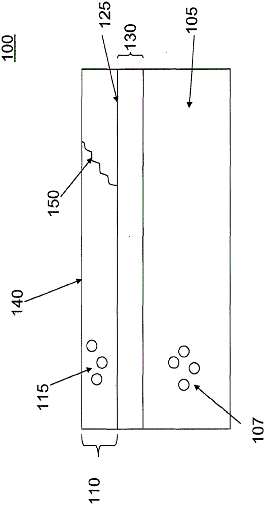
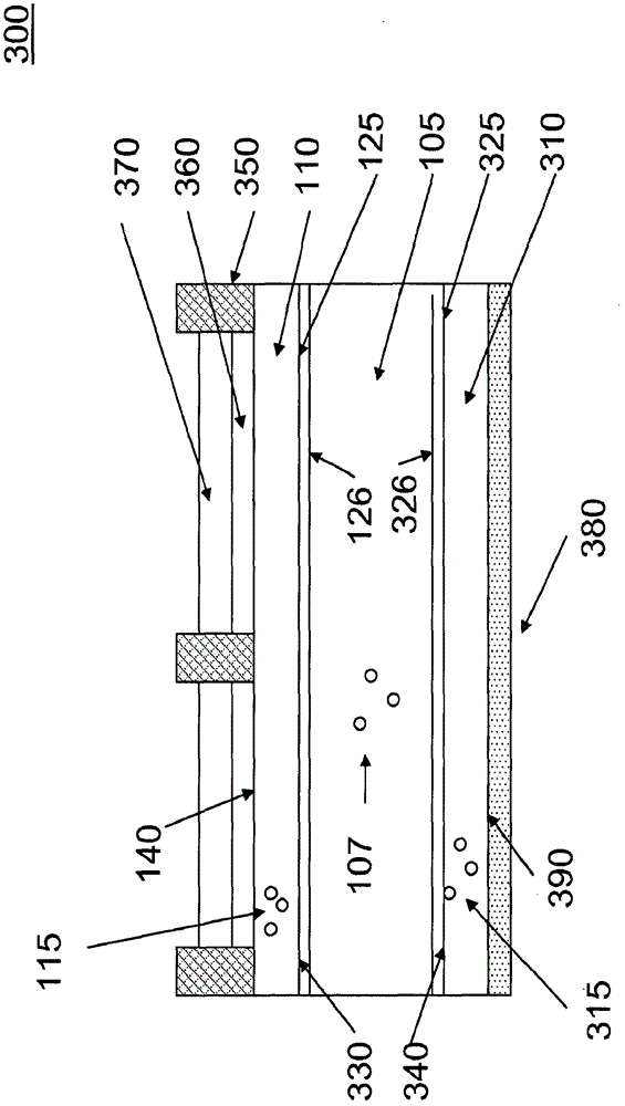
[0039] Various device structures including semiconductor substrates are described. An amorphous semiconductor layer is deposited on the surface of the first substrate and annealed at a temperature sufficient to crystallize the amorphous layer but equal to or less than 700C. In a preferred embodiment, the passivation and anti-reflection coatings are deposited at or below 700C, as are the metal electrodes in contact with the semiconductor surface, resulting in a device capable of detecting electromagnetic radiation. The substrate 105 may comprise a single crystal or polycrystalline semiconductor wafer, or a thin film semiconductor residing on a heterogeneous substrate (material) such as glass, quartz, metal, graphite, plastic, metallurgical grade silicon Or ceramics. In alternative embodiments, the substrate 105 may be silicon, silicon on glass, silicon on sapphire, silicon on quartz, silicon on metal, silicon on graphite, silicon on ceramic, a compound of silicon and germanium...


PUM


Abstract

A semiconductor is disclosed with a substrate doped with a substrate doping. There is a crystalline semiconductor layer disposed on a front side of the substrate. The crystalline semiconductor layer has a layer doping. The substrate doping changes to the layer doping within a 100 angstrom transition region. In alternative embodiments, the layer doping has novel profiles. In other alternative embodiments, the substrate has a crystalline semiconductor layers disposed on each of a front and a back side of the substrate. Each of the crystalline semiconductor layers has a respective layer doping and each of these layer dopings changes to the substrate doping within a respective transition region less than 100 angstroms thick. In still other embodiments of this invention, an amorphous silicon layer is disposed on a side of the crystalline semiconductor layer opposite the substrate.; The amorphous silicon layer has an amorphous doping so that a tunnel junction is formed between the doped crystalline semiconductor layer and the amorphous layer. Manufacturing these structures at below 700 degrees Centigrade enables the narrow transition regions of the structures.

Description

[0001] Cross References to Related Applications [0002] This application is related to an application entitled "Method of Making a Semiconductor Optical Detector Structure" filed on the same date by the same inventor as this application, the entire contents of which are hereby incorporated by reference. [0003] This application claims priority to Provisional Patent Application Serial No. 61 / 219,131, filed June 22, 2009, entitled "Low Cost, Low Thermal Budget Solar Cells." technical field [0004] The present invention relates to semiconductor optical detector structures. More particularly, the present invention relates to low temperature fabricated solar cell structures. Background technique [0005] Solar cells are a promising approach to enhancing the world's energy supply. Silicon-based solar cells are currently the dominant photovoltaic technology. Silicon solar cells can be produced starting from semiconductor wafers, wherein the semiconductor wafers can consist of...

Claims


Application Information

Patent Timeline
Patent Type & Authority Applications(China)
IPC IPC(8): H01L31/0368H01L31/0392H01L31/072H01L31/18H01L31/068H01L31/078
CPCH01L31/1804H01L31/1872H01L31/068H01L31/03921Y02E10/548H01L31/078Y02E10/547Y02P70/50
Inventor J·德·索扎H·豪威尔D·因斯金志焕D·萨达纳
Owner IBM CORP
Why Eureka
Try Eureka