Semiconductor device and method for forming same

A semiconductor and device technology, which is applied in the field of semiconductor devices including metal gates and their formation, can solve the problems of increased resistance of conductive plugs, poor conductivity of metal gate surfaces, and easy oxidation of the top of metal gates, etc., to achieve The effect of reducing resistance, improving reliability and electrical performance, and preventing deterioration of electrical conductivity

Active Publication Date: 2015-04-01
SEMICON MFG INT (SHANGHAI) CORP
View PDF6 Cites 0 Cited by
  • Summary
  • Abstract
  • Description
  • Claims
  • Application Information

AI Technical Summary

Problems solved by technology

[0004] In practical applications, it is found that the top of the metal gate in the semiconductor device formed by the above technical solution is easily oxidized, resulting in poor conductivity of the surface of the metal gate, which in turn increases the resistance of the conductive plug connected to the metal gate.

Method used


Image

  • Semiconductor device and method for forming same
  • Semiconductor device and method for forming same
  • Semiconductor device and method for forming same

Examples


Embodiment approach

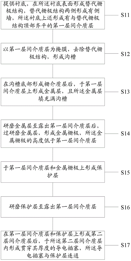
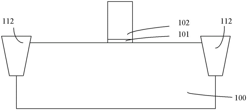
[0014] In order to solve the above problems, the present invention provides a specific implementation method for forming a semiconductor device including a metal gate, the specific process is as follows: perform step S11, provide a substrate, form a replacement gate structure on the surface of the substrate, and replace the gate structure Side walls are formed on both sides, and a first interlayer dielectric layer flush with the top of the replacement gate structure is also formed on the substrate; step S12 is performed, using the first interlayer dielectric layer as a mask to remove the replacement gate structure, forming a trench; perform step S13, after forming a gate dielectric layer at the bottom of the trench, form a metal layer on the first interlayer dielectric layer, and the metal layer fills the trench; perform step S14, grind the metal layer to After exposing the first interlayer dielectric layer, grind the metal layer to form a metal gate, the height of the metal ga...


PUM


Abstract

The invention provides a semiconductor device and a method for forming the same. The semiconductor device comprises a substrate, a first interlayer dielectric layer, a metal grid, side walls, a second interlayer dielectric layer and a conductive plug, wherein the first interlayer dielectric layer is positioned on the substrate; the metal grid is positioned on the substrate and is formed in the first interlayer dielectric layer; the side walls are positioned on the substrate and are arranged on two sides of the metal grid; the second interlayer dielectric layer is positioned on the first interlayer dielectric layer and covers the metal grid and the side walls; the conductive plug is positioned in the second interlayer dielectric layer; and a protecting layer is arranged between the metal grid and the second interlayer dielectric layer and is communicated with the conductive plug. The phenomenon that the surface conductivity of the metal grid becomes poor so that the resistance of the conductive plug connected with the metal grid is reduced is effectively prevented, and the reliability and the electrical property of the semiconductor device are improved.

Description

technical field [0001] The invention relates to the field of semiconductor technology, in particular to a semiconductor device including a metal gate and a forming method thereof. Background technique [0002] With the continuous improvement of the integration level of semiconductor devices and the reduction of technology nodes, the traditional gate dielectric layer continues to become thinner, and the leakage of transistors increases accordingly, causing problems such as waste of power consumption of semiconductor devices. In order to solve the above problems, the prior art provides a solution of replacing the polysilicon gate with a metal gate. Among them, the "gate last" process is a main process for forming the metal gate. [0003] In U.S. Patent No. 6,664,195, a method for forming a semiconductor device including a metal gate using a "gate-last" process is provided, including: providing a semiconductor substrate on which a replacement gate structure is formed and locat...

Claims


Application Information

Patent Timeline
Patent Type & Authority Patents(China)
IPC IPC(8): H01L21/336H01L21/28H01L21/768H01L29/78H01L29/49
Inventor 王新鹏
Owner SEMICON MFG INT (SHANGHAI) CORP
Why Eureka
Try Eureka