Phase-changing memory unit with similar super lattice structure and preparation method thereof

A phase change storage and superlattice technology, applied in the field of microelectronics, can solve the problems of slow phase change, poor thermal stability and data retention, and large operating current, so as to improve stability and facilitate precise control of super Lattice structure and subsequent process, the effect of reducing "write" current and power consumption

Inactive Publication Date: 2012-12-05
SHANGHAI INST OF MICROSYSTEM & INFORMATION TECH CHINESE ACAD OF SCI
View PDF2 Cites 14 Cited by
  • Summary
  • Abstract
  • Description
  • Claims
  • Application Information

AI Technical Summary

Problems solved by technology

[0006] In view of the shortcomings of the prior art described above, the object of the present invention is to provide a phase-change memory unit with a superlattice-like structure and a preparation method thereof, which are used to solve the thermal stability of the phase-change memory unit in the prior art. Poor performance and data retention, slow phase transition and high operating current

Method used


Image

  • Phase-changing memory unit with similar super lattice structure and preparation method thereof
  • Phase-changing memory unit with similar super lattice structure and preparation method thereof
  • Phase-changing memory unit with similar super lattice structure and preparation method thereof

Examples


Embodiment 1

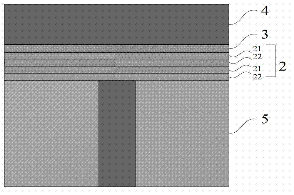
[0048] see figure 1 Shown, a kind of phase-change memory unit, it comprises lower electrode 1, the dielectric layer 5 that wraps lower electrode 1, the phase-change material layer 2 that is positioned at dielectric layer 5, is positioned at this phase-change material layer 2 heating layer 3 and is positioned at The electrode 4 on the heating layer 3. The phase change material layer is composed of a single layer of GaSb and a single layer of phase change material Sb 2 Te 3 A superlattice-like structure formed by alternating periodic growth of monolayers with nanometer thickness. The phase-change material layer 2 (that is, the superlattice-like structure includes a single-layer GaSb layer 21, a single-layer phase-change material Sb layer on the single-layer GaSb layer 21 2 Te 3 Layer 22, located in the single layer phase change material Sb 2 Te 3 The single-layer GaSb layer 21 on the layer 22...and so on, the structure can be repeated periodically until the thickness of the...

Embodiment 2

[0061] In this embodiment, Step 1 and Step 3 are the same as Embodiment 1. Also includes the following steps:

[0062] Step 4: Set the RF power corresponding to the GaSb alloy target to 25 watts, the Ar flow rate to 20 SCCM, and wait until the background vacuum is lower than 3×10 -4 Pascal, turn on the RF power supply, open the Ar inlet valve, open the GaSb alloy target cover and count the time, after 80 seconds of sputtering, turn off the GaSb alloy target RF power supply and the target cover, the thickness of the single-layer GaSb sputtered this time is 4nm.

[0063] Step 5: Add Sb 2 Te 3 The radio frequency power corresponding to the alloy target is set to 20 watts, the Ar flow rate is set to 20 SCCM, and the background vacuum is lower than 3×10 -4 Pascal, turn on the RF power, open the Ar inlet valve, open the Sb 2 Te 3 The alloy target is covered and timed. After 60 seconds of sputtering, the GaSb alloy target RF power supply and the target cover are turned off. The ...


PUM

PropertyMeasurementUnit
thicknessaaaaaaaaaa
thicknessaaaaaaaaaa
thicknessaaaaaaaaaa

Abstract

The invention provides a phase-changing memory unit with a similar super lattice structure, which comprises a phase-changing material layer. In the phase-changing material layer, the similar super lattice structure is formed by periodic and alternate growth of a single GaSb layer and a single phase-changing material Sb2Te3 layer in a nano-thick single layer. The single GaSb layer is 2-8nm thick, and the single phase-changing material Sb2Te3 is 3-12nm thick. The similar super lattice material has the advantages of adjustable crystallization temperature, low thermal conductivity, good thermal stability and high phase-changing speed. When the similar super lattice material is applied in a phase-changing memory, the phase-changing memory has the advantages of high data retention capability, high erasing and writing speed and low power consumption. A particularly preferred similar super lattice GaSb (4 nm) / Sb2Te3 (6nm) has more advantages than other components in the performance of materials and devices.

Description

technical field [0001] The invention belongs to the technical field of microelectronics, and relates to a low-power phase-change storage unit in the technical field of microelectronics and a preparation method thereof, in particular to a phase-change storage unit with a superlattice-like structure and a preparation method thereof. Background technique [0002] Compared with the mainstream semiconductor storage technology in the market, phase change memory has many advantages, such as high density, low power consumption, fast operation, long cycle life, etc., especially in terms of device feature size reduction. Therefore, phase change memory is considered to be one of the best solutions for the next generation of non-volatile memory technology, and has broad commercial prospects in terms of high density, high speed, low voltage, low power consumption and embedded storage. [0003] Phase change memory uses chalcogenide compounds as the storage medium. The Joule heat generated...

Claims


Application Information

Patent Timeline
Patent Type & Authority Applications(China)
IPC IPC(8): H01L45/00B82Y10/00
Inventor 吕业刚宋三年宋志棠吴良才饶峰刘波
Owner SHANGHAI INST OF MICROSYSTEM & INFORMATION TECH CHINESE ACAD OF SCI
Why Eureka
Try Eureka