Detection pulse generator, control chip and switching power source
A technology for detecting pulses and switching power supplies, applied to electrical components, output power conversion devices, and conversion equipment without intermediate conversion to AC, to achieve the effect of reducing output voltage undershoot and improving system efficiency
- Summary
- Abstract
- Description
- Claims
- Application Information
AI Technical Summary
Problems solved by technology
Method used
Image

Examples
Embodiment 1
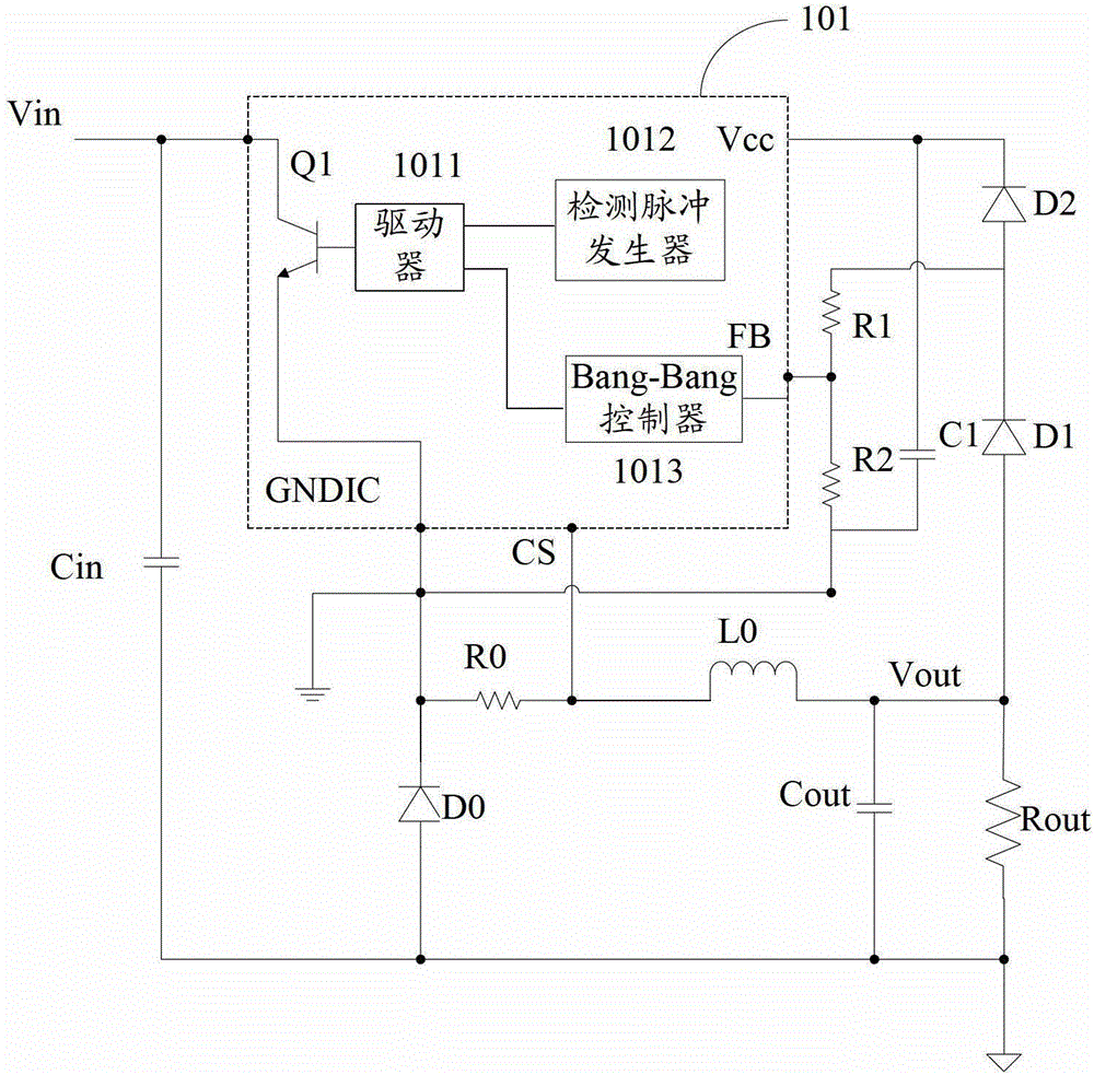
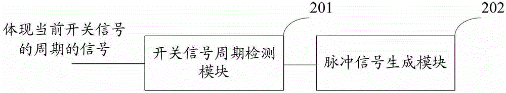
[0053] Please refer to the attached figure 2 , is a schematic structural diagram of the first detection pulse generator disclosed in the embodiment of the present invention. This circuit is applied to a switching power supply controlled by Bang-Bang. The circuit may include: a switching signal cycle detection module 201 and a detection pulse generation module 202, wherein :
[0054] The signal representing the period of the current switch signal acts on an input terminal of the switch signal period detection module 201 , and the output terminal of the switch signal period detection module 201 is connected to the input terminal of the detection pulse generation module 102 .
[0055] It works as follows:
[0056] The switch signal period detection module 201 generates an equivalent switch period signal with the same period as the current switch signal according to the signal reflecting the period of the current switch signal. When the detection pulse generation module 202 dete...
Embodiment 2
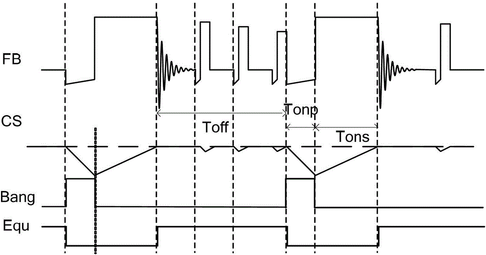
[0061]At the beginning, the switching power supply first generates a detection pulse. When it is detected that the output voltage of the switching power supply is lower than the preset lower limit voltage, a switching signal is generated. Therefore, the detection pulse is generated first, and then the switching signal is generated. The above-mentioned embodiments only illustrate The detection pulse generation process after the first switch signal is generated does not illustrate the generation process of the detection pulse before the first switch signal is generated. Of course, the generation process of the detection pulse before the first switch signal can be compared with the prior art The process of generating the pulse is the same as in the prior art, so it is not repeated here one by one. The generation process of the detection pulse before the generation of the first switching signal can also be described as follows.
[0062] The embodiment of the present invention also...
Embodiment 3
[0076] In practical applications, there are many ways to implement each module in Embodiment 2, and each module will be introduced in detail below.
[0077] see Figure 4 , which is a circuit diagram of a detection pulse generation module provided in an embodiment of the present invention, the detection pulse generation module may include:
[0078] Oscillator 401, counter 402, encoder 403, first AND gate 404, D flip-flop 405, multiplexer 406, second AND gate 407 and trigger unit 408;
[0079] The output terminal of the oscillator 401 is connected with the clock input terminal Clk of the counter 402, the output terminal of the counter 402 is respectively connected with the input terminal of the multiplexer 406 one-to-one, and the output terminal of the counter 402 is connected with the input terminal of the encoder 403 respectively. Connected to one, the set signal acts on the set terminal S of the counter 402 and an input terminal of the first AND gate 404 respectively, the r...
PUM
 Abstract
Description
Claims
Application Information
 - R&D
- Intellectual Property
- Life Sciences
- Materials
- Tech Scout
- Unparalleled Data Quality
- Higher Quality Content
- 60% Fewer Hallucinations
Browse by: Latest US Patents, China's latest patents, Technical Efficacy Thesaurus, Application Domain, Technology Topic, Popular Technical Reports.
© 2025 PatSnap. All rights reserved.Legal|Privacy policy|Modern Slavery Act Transparency Statement|Sitemap|About US| Contact US: help@patsnap.com