
Method for manufacturing flexible IGZO (In-Ga-Zn-O) thin film transistor

A thin-film transistor and flexible technology, applied in the field of microelectronics, can solve the problems that cannot be copied to flexible substrates, and the insulating layer cannot be prepared under the optimal process (300℃-350℃)

Inactive Publication Date: 2012-12-19
GUANGDONG SINODISPLAY TECH
View PDF5 Cites 9 Cited by
  • Summary
  • Abstract
  • Description
  • Claims
  • Application Information

AI Technical Summary

Problems solved by technology

This determines that the deposition process on the hard substrate cannot be simply copied to the flexible substrate.
For plastic substrates, they usually cannot withstand high temperatures of 300°C. This shortcoming determines that the insulating layer cannot be prepared under the optimal process (300°C-350°C), and it is impossible to obtain stable device performance by annealing at high temperatures. Optimize the device structure, material, and deposition process to obtain TFT devices with better performance

Method used

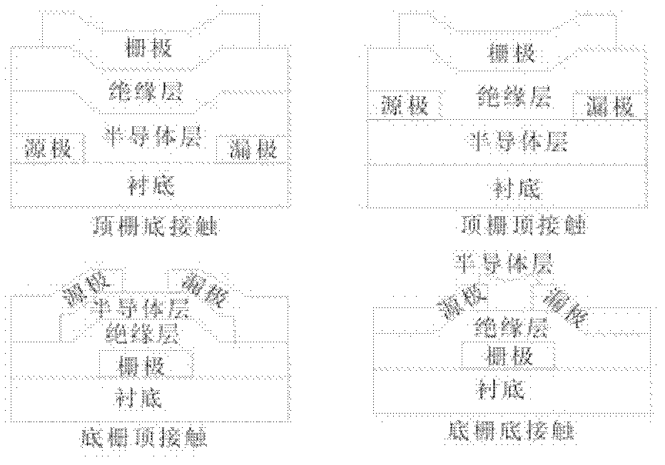
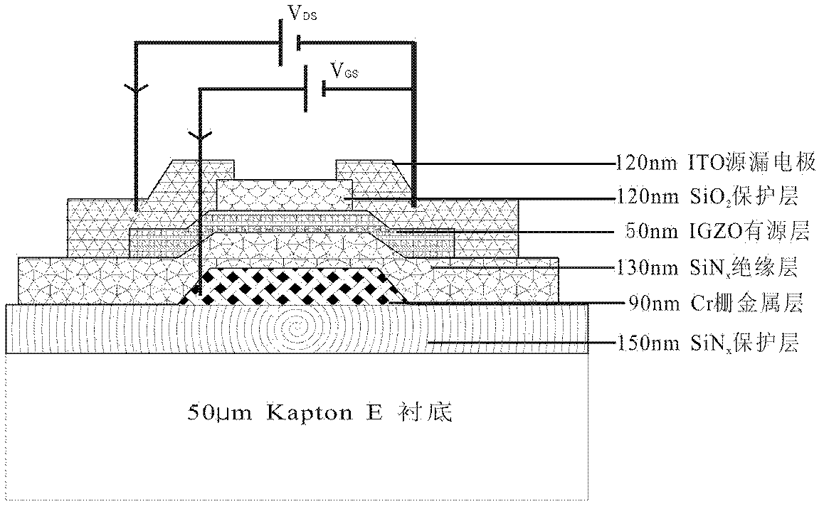

Image

  • Method for manufacturing flexible IGZO (In-Ga-Zn-O) thin film transistor
  • Method for manufacturing flexible IGZO (In-Ga-Zn-O) thin film transistor
  • Method for manufacturing flexible IGZO (In-Ga-Zn-O) thin film transistor

Examples


Embodiment Construction

[0047] A flexible IGZO thin film transistor provided by the present invention will be described in detail below with reference to the drawings and specific embodiments.

[0048] Fabrication and Characterization of Thin Film Layer of Flexible IGZO-TFT Device Structure

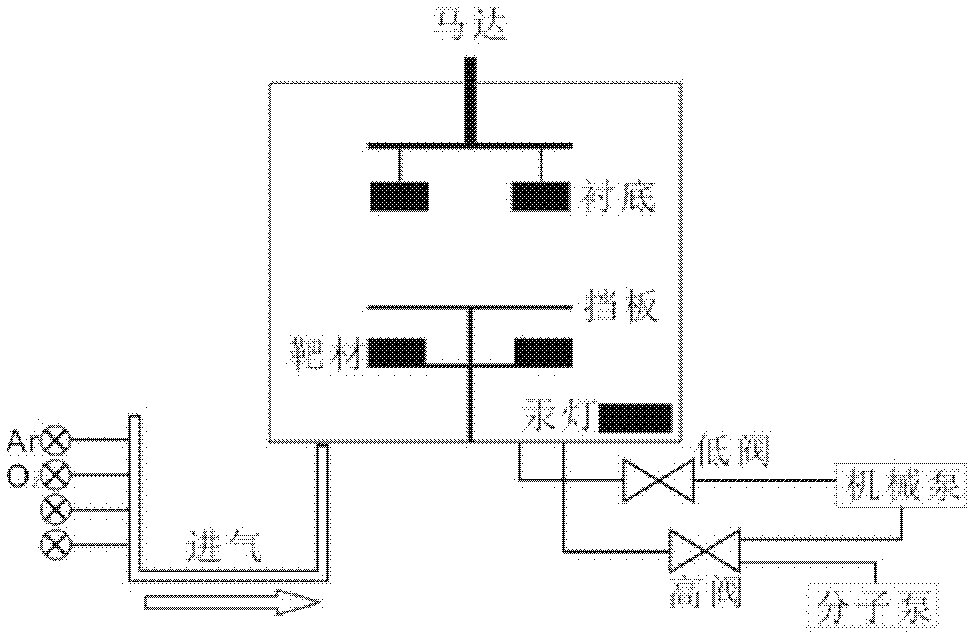
[0049] The goal of this application is to find a suitable flexible substrate, explore the thin film materials and preparation technology of each layer of TFT, and realize the three-primary-color-driven microcapsule display unit by making and testing the electrical properties of IGZO-TFT device samples, analyzing and continuously improving the process parameters The required TFT device, the above work involves equipment including magnetron sputtering system, plasma enhanced chemical vapor deposition (PECVD) system and reactive ion etching (RIE) system, etc., which will be introduced in detail below.

[0050] Magnetron sputtering system

[0051] In this work, the gate electrode, source-drain electrode and semicon...


PUM


Abstract

The invention provides a method for manufacturing a flexible IGZO (In-Ga-Zn-O) thin film transistor. The method comprises the following steps: step one, cleaning a flexible substrate; step two, depositing SiNx isolating layer by using PECVD (Plasma Enhanced Chemical Vapor Deposition); step three, preparing a gate electrode pattern; step four, preparing a gate insulating layer; step five, preparing an IGZO semiconductor layer; step six, preparing a source drain electrode; and step seven, preparing a protection layer. As the deposition temperature is reduced, and the deposition power of the protection layer and the thickness of a silicon nitride insulating layer are optimized, a flexible IGZO-TFT (Thin Film Transistor) device is manufactured successfully, the performances of the flexible IGZO-TFT are as follows: the threshold voltage is 8V, the switching ratio is 5*107, the saturated migration rate is 7.8cm2 / V.s, and the subthreshold slope factor is 0.9V / dec; the device is arranged on a cylinder with the curvature radius being 10mm is bent for 3 minutes, and the performances can not be changed basically; and the protection layer plays an important role in the stability of the device.

Description

technical field [0001] The invention relates to the technical field of microelectronics, and more specifically, relates to a method for manufacturing an IGZO (In-Ga-Zn-O) thin film transistor. Background technique [0002] TFT-LCD is widely used in various large, medium and small size products due to its advantages of thin size, light weight, excellent picture quality, low power consumption, long life, digitalization and no radiation, almost covering today's information The main electronic products of society, such as TV, computer (desktop and notebook), mobile phone, PDA, GPS, vehicle display, instrumentation, public display and virtual display, etc. At the 2007 Display Search China FPD Conference (2007 Display Search China FPD Conference), the industry generally believed that any kind of flat panel display technology in the next ten years It will not be able to replace the dominant position of TFT-LCD in the field of flat panel display within this year, and globally, the ...

Claims


Application Information

Patent Timeline
Patent Type & Authority Applications(China)
IPC IPC(8): H01L21/336G01R31/26
Inventor 王彬
Owner GUANGDONG SINODISPLAY TECH
Learn More