
SCR (silicon controlled rectifier) type LDMOS ESD (lateral double diffusion metal-oxide-semiconductor device electrostatic discharge) device

A device and well region technology, applied in semiconductor devices, electrical components, circuits, etc., can solve the problems of low ESD protection level and small discharge current per unit area, and achieve high ESD protection level, adjustable trigger voltage, and electrostatic discharge current. increased effect

Active Publication Date: 2012-12-19
PEKING UNIV
View PDF6 Cites 11 Cited by
  • Summary
  • Abstract
  • Description
  • Claims
  • Application Information

AI Technical Summary

Problems solved by technology

[0020] The technical problem to be solved in the present invention is: how to design a kind of LDMOS ESD device, to solve the problems of small discharge current per unit area and low ESD protection level of existing LDMOS ESD devices

Method used


Image

  • SCR (silicon controlled rectifier) type LDMOS ESD (lateral double diffusion metal-oxide-semiconductor device electrostatic discharge) device
  • SCR (silicon controlled rectifier) type LDMOS ESD (lateral double diffusion metal-oxide-semiconductor device electrostatic discharge) device
  • SCR (silicon controlled rectifier) type LDMOS ESD (lateral double diffusion metal-oxide-semiconductor device electrostatic discharge) device

Examples


Embodiment Construction

[0039] The specific implementation manners of the present invention will be further described in detail below in conjunction with the accompanying drawings and embodiments. The following examples are used to illustrate the present invention, but are not intended to limit the scope of the present invention.

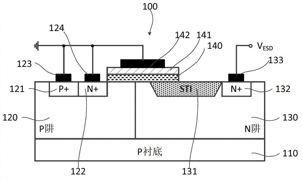
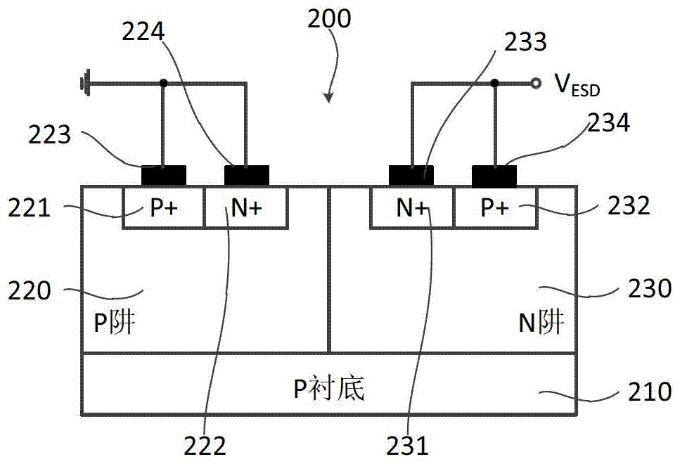
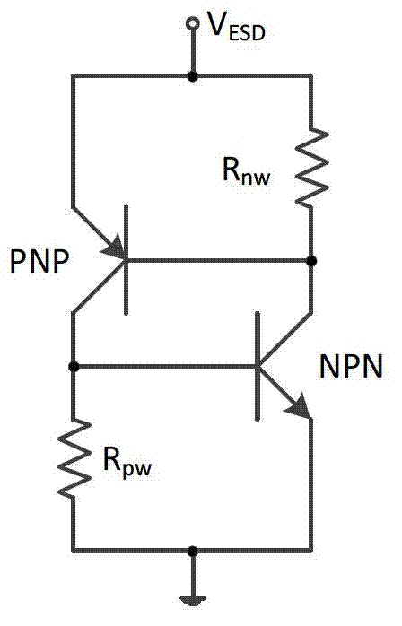
[0040] The core idea of ​​the present invention is to provide an SCR type LDMOS ESD device, in which a P+ doped region is provided in the N well region of the SCR type LDMOS ESD device, so that a parasitic SCR transistor is formed on the back of the SCR type LDMOS ESD device. When the ESD impact occurs, the parasitic SCR transistor acts as the main electrostatic discharge device, so that the electrostatic discharge current per unit area of ​​the SCR type LDMOS ESD device increases, thereby obtaining a high ESD protection level. The trigger voltage of the SCR type LDMOS ESD device is determined by the length of the drift region of the LDMOS transistor, and the trigger voltage...


PUM


Abstract

The invention relates to the technical field electrostatic discharge protection of an integrated circuit and discloses an SCR (silicon controlled rectifier) type LDMOS ESD (lateral double diffusion metal-oxide-semiconductor device electrostatic discharge) device. A P+doping region is arranged at an N-well region of the SCR type LDMOS ESD device, so that a parasitic SCR transistor is arranged at the back side of the SCR type LDMOS ESD device. When the ESD impact happens, the parasitic SCR transistor is used as a main electrostatic discharge device, so that the unit area electrostatic discharge current of the SCR type LDMOS ESD device is increased, and a high ESD protection level is obtained; in addition, the triggering voltage of the SCR type LDMOS ESD device is determined by a drift region length of an LDMOS transistor, and the regulation of the triggering voltage is realized.

Description

technical field [0001] The invention relates to the technical field of electrostatic discharge protection of integrated circuits, in particular to an SCR type LDMOS ESD device. Background technique [0002] The electrostatic discharge (ESD) phenomenon of integrated circuits is a transient process in which a large amount of charge is poured into the integrated circuit from the outside to the inside when the chip is floating. Since the internal resistance of the integrated circuit chip is very low, when the ESD phenomenon occurs, an instantaneous (taking 100-200 nanoseconds, rising time is only about 0.1-10 nanoseconds), high peak (several amperes) current will be generated, and A large amount of Joule heat is generated, which will cause the failure of the integrated circuit chip. [0003] For high-voltage power integrated circuits, Lateral Double Diffusion Metal-Oxide-Semiconductor (LDMOS) transistors are widely used as protection devices for high-voltage input / output pins d...

Claims


Application Information

Patent Timeline
IPC IPC(8): H01L29/06H01L29/78
Inventor 王源张鹏曹健陆光易贾嵩张兴
Owner PEKING UNIV
Learn More