Double-heterostructure GaN-based high-electron mobility transistor structure and preparation method

A high electron mobility, double heterostructure technology, applied in semiconductor/solid state device manufacturing, circuits, electrical components, etc., can solve problems such as reducing electron mobility and controversy

Active Publication Date: 2012-12-26
INST OF SEMICONDUCTORS - CHINESE ACAD OF SCI
View PDF2 Cites 8 Cited by
  • Summary
  • Abstract
  • Description
  • Claims
  • Application Information

AI Technical Summary

Problems solved by technology

However, replacing the high-resistance gallium nitride buffer layer with an aluminum gallium nitride high-resistance buffer layer, although the aluminum composition is very low (generally below 5%), it will still greatly reduce the electron mobility. Using gallium nitride as the high-resistance The high electron mobility transistor material developed by the buffer layer, the room te

Method used


Image

  • Double-heterostructure GaN-based high-electron mobility transistor structure and preparation method
  • Double-heterostructure GaN-based high-electron mobility transistor structure and preparation method

Examples


Embodiment Construction

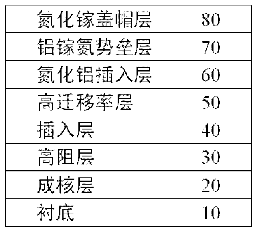
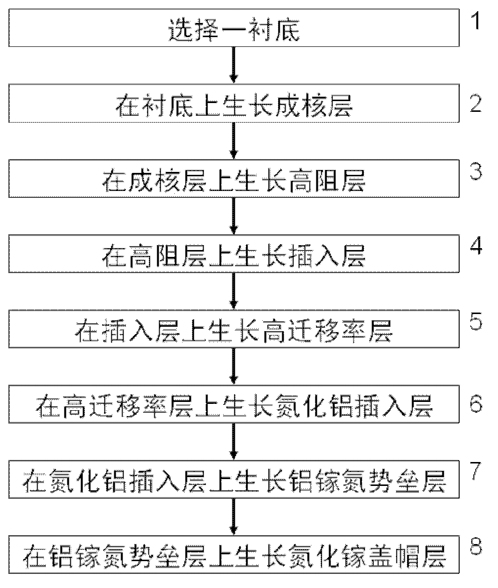
[0027] see figure 1 As shown, a double heterostructure GaN-based high electron mobility transistor structure of the present invention includes:

[0028] a substrate 10;

[0029] A nucleation layer 20, the nucleation layer 20 is fabricated on the substrate 10, the nucleation layer 20 is gallium nitride or aluminum nitride or aluminum gallium nitride, with a thickness of 0.01-0.50 μm.

[0030] An unintentionally doped high-resistance layer 30, the unintentionally doped high-resistance layer 30 is fabricated on the nucleation layer 20, and the material of the unintentionally doped high-resistance layer 30 is Al y Ga 1-y N, where 06 Ω.cm. The high-resistance layer 30 has four functions, one is to reduce the lattice mismatch between the substrate and the epitaxial layer as a buffer layer, and improve the crystal quality of the epitaxial layer; the other is to reduce device leakage as a high-resistance layer; It is used as the back barrier layer to raise the barrier height of th...


PUM

PropertyMeasurementUnit
Thicknessaaaaaaaaaa
Thicknessaaaaaaaaaa
Thicknessaaaaaaaaaa

Abstract

A double-heterostructure GaN-based high-electron mobility transistor structure comprises: a substrate; a nucleating layer prepared on the substrate; an unpurposed doped high resistance layer prepared on the nucleating layer; an unpurposed doped inserting layer prepared on the unpurposed doped high resistance layer; an unpurposed doped high mobility layer prepared on the unpurposed doped inserting layer; an unpurposed doped aluminum nitride inserting layer prepared on the high mobility layer; an unpurposed doped ALGaN barrier layer prepared on the unpurposed doped aluminum nitride inserting layer; and an unpurposed doped GaN capping layer prepared on the unpurposed doped ALGaN barrier layer.

Description

technical field [0001] The invention belongs to the technical field of semiconductors, in particular to a double-heterostructure gallium nitride-based high electron mobility transistor structure and manufacturing method, the transistor uses high resistance aluminum gallium nitrogen with low aluminum composition as a buffer layer, and A thin aluminum nitride insertion layer is introduced on both sides of the gallium nitride channel layer. The high-resistance aluminum gallium nitride as a buffer layer can reduce the leakage of channel electrons in the buffer layer and improve the breakdown voltage of the device. The thin aluminum nitride insertion layer can Reduce the alloy scattering of electrons and improve the channel electron mobility. Background technique [0002] As a typical representative of the third-generation wide-bandgap semiconductor, gallium nitride has excellent physical and chemical properties, and is very suitable for the development of high-frequency, high-vo...

Claims


Application Information

Patent Timeline
IPC IPC(8): H01L29/778H01L29/06H01L21/335
Inventor 王晓亮王翠梅肖红领彭恩超冯春姜丽娟陈竑
Owner INST OF SEMICONDUCTORS - CHINESE ACAD OF SCI
Why Eureka
Try Eureka