Coupling aligning device for waveguide chip and photo-diode (PD) array and aligning method applying coupling aligning device

A waveguide chip and alignment device technology, which is applied in the field of communication, can solve the problems of destroying high-frequency characteristics, the speed cannot meet the requirements, etc., and achieve the effect of fast operation, simple coupling and alignment, and high alignment accuracy

Inactive Publication Date: 2013-01-09
GUANGXUN SCI & TECH WUHAN
View PDF7 Cites 26 Cited by
  • Summary
  • Abstract
  • Description
  • Claims
  • Application Information

AI Technical Summary

Problems solved by technology

However, for 100G receivers, this alignment method has the following disadvantages: 1) The four-group PD array used in 100G receivers needs to monitor four electrical signals at the same time when using active alignment, while the coupling pair There are 6 dimensions that need to be adjusted on time, and it is not an easy task to ensure that the photocurrent reaches the maximum value at the same time through 6-dimensional adjustment
2) The photocurrent needs to be monitored during active alignment. To monitor the photocurrent, an additional gold wire must be drawn from the gold-plated pad on the PD for detection by the picoammeter. For high-frequency circuits, this method of extra-leading the test line will Destroy its high-frequency characteristics until its rate cannot reach the required 25Gbps

Method used


Image

  • Coupling aligning device for waveguide chip and photo-diode (PD) array and aligning method applying coupling aligning device
  • Coupling aligning device for waveguide chip and photo-diode (PD) array and aligning method applying coupling aligning device
  • Coupling aligning device for waveguide chip and photo-diode (PD) array and aligning method applying coupling aligning device

Examples


Embodiment Construction

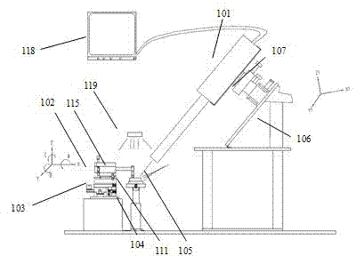
[0038] The present invention will be described below in conjunction with the drawings, such as figure 1 , figure 2 As shown, the active optical alignment device for the coupling of the waveguide chip and the high-speed PD array of the present invention includes: a set of infrared CCD monitoring system whose response spectrum covers visible light and near-infrared light bands, infrared CCD (Charge Coupled Device, Charge coupling device) monitoring system consists of infrared CCD101, three-dimensional fine-tuning frame 107, infrared CCD bracket 106 and monitor 118. The infrared CCD monitoring system is used to observe the position of the light-sensitive surface of the PD array and the output spot of the waveguide chip. At this time, infrared CCD101 needs Tilt and align the PD array 108; a six-dimensional fine-tuning frame 103 is provided with a clamping unit 102, and the clamping unit 102 is fixed with a waveguide support frame 115; besides the six-dimensional fine-tuning frame 10...


PUM


Abstract

The invention provides a coupling aligning method for a waveguide chip and a photo-diode (PD) array. An infrared light source is adopted for lighting, so that the PD array is clearly imaged in a monitoring instrument through an infrared charge coupled device (CCD); a fine adjustment frame is adjusted to control the heights and the horizontal positions of the waveguide chip and the PD array, so that a light spot reflected by the waveguide chip perpendicularly drops on a PD photosensitive surface, and further high-efficiency coupling is achieved, or a driving module is connected with a computer to automatically adjust a six-dimensional fine adjustment frame; the computer acquires infrared CCD image information through a data acquisition card; automatic control software processes an image to obtain a light spot array reflected by the waveguide chip and a slope and a position difference of a PD photosensitive surface array; the automatic control software controls an axial direction adjusted to the six-dimensional fine adjustment frame, so that the light spot array is superposed with the PD photosensitive surface array. The invention also provides a coupling aligning device for the waveguide chip and the PD array. By the method and the device, the alignment time of the waveguide chip and the PD array can be shortened, and the alignment efficiency and the repetitiveness are improved, so that the consistency of a product is guaranteed.

Description

Technical field [0001] The invention relates to a hybrid integration method of an optical transmission medium and a semiconductor optoelectronic device in the optical communication field, and particularly relates to an optical alignment device and an alignment method between an optical waveguide chip and a photodetecting device. The invention belongs to the communication field. [0002] Background technique [0003] The optical communication technology is developing day by day, and its transmission rate is constantly increasing. At present, 40G technology has matured, and the future development direction of 40G technology is to gradually reduce equipment costs. In the next few years, 100G technology will gradually replace 40G technology and become the mainstream high-speed new transmission commercial technology. The speed is constantly increasing, but the nature of the communication system has not changed. The optical communication system consists of a data source, an optical tra...

Claims


Application Information

Patent Timeline
Patent Type & Authority Applications(China)
IPC IPC(8): G02B6/43
Inventor 石川梁雪瑞陈征江雄赵小博汪灵杰
Owner GUANGXUN SCI & TECH WUHAN
Why Eureka
Try Eureka