

Light-emitting diode encapsulating structure and manufacturing method thereof
A technology for light-emitting diodes and packaging structures, which is applied to electrical components, electrical solid-state devices, circuits, etc., can solve the problems of wire falling off, the complicated and tedious process of bonding and bonding, and affecting the production yield of light-emitting diode packaging structures, so as to facilitate heat dissipation. , the effect of the production process is simple
- Summary
- Abstract
- Description
- Claims
- Application Information
AI Technical Summary
Problems solved by technology
Method used
Image

Examples
Embodiment Construction
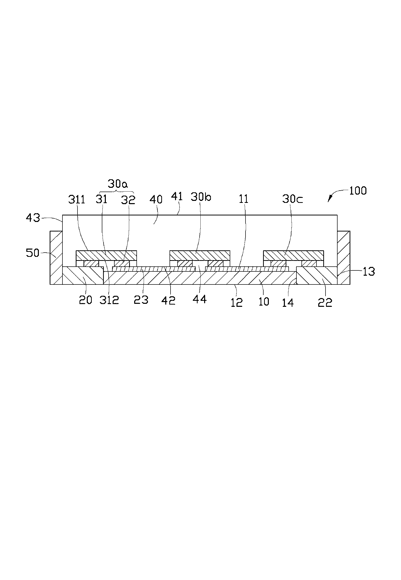
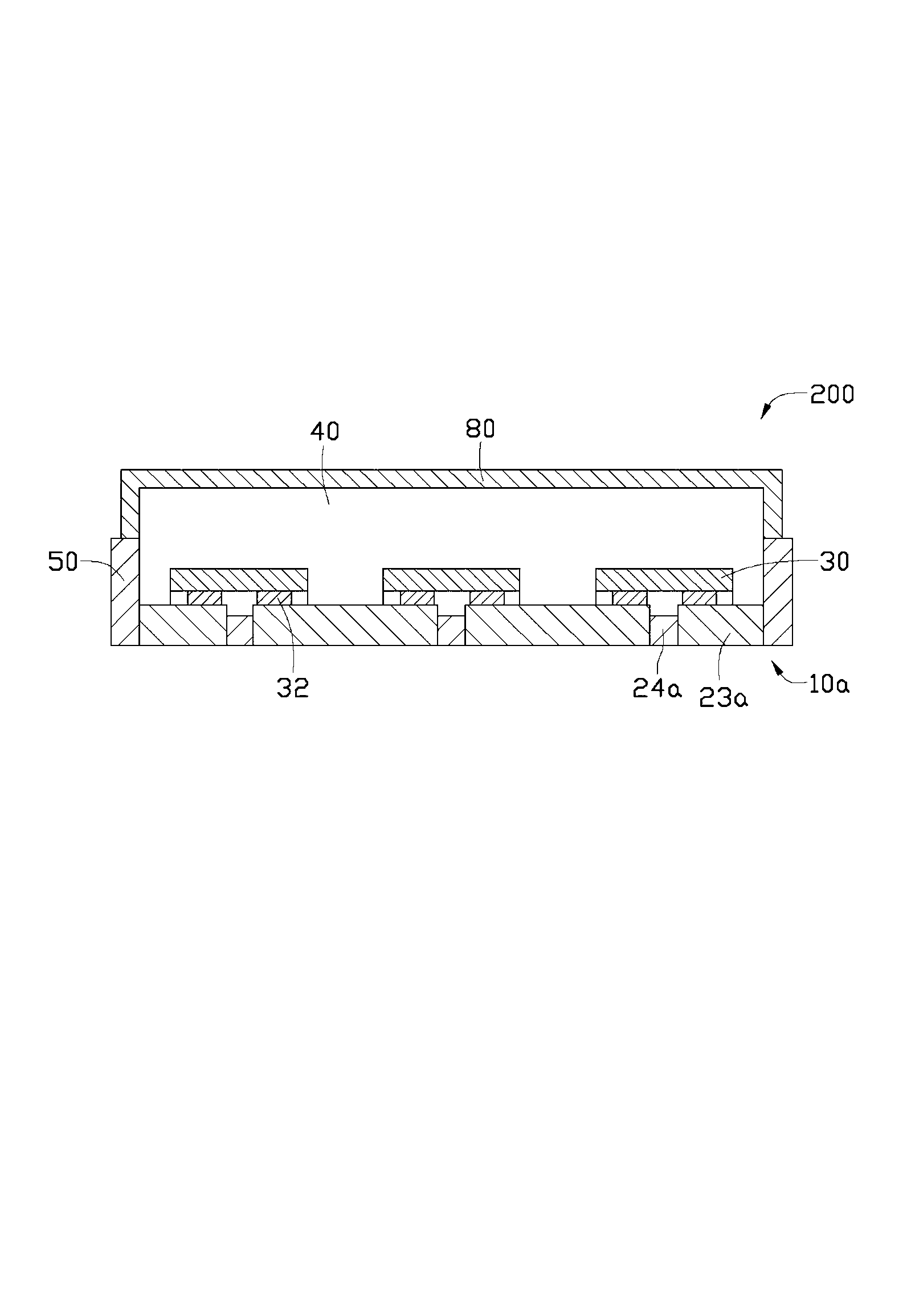
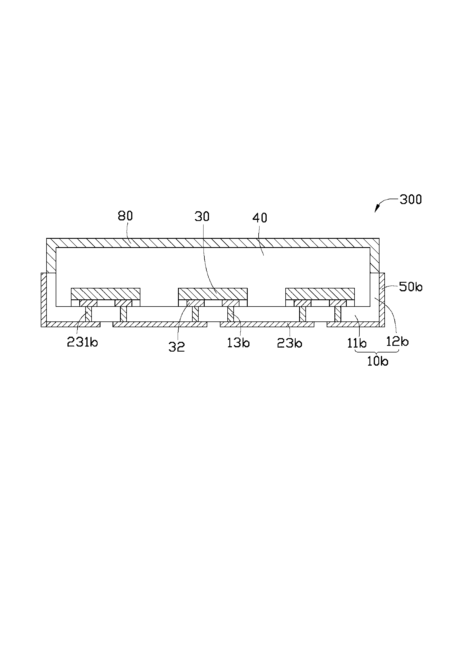
[0021] See figure 1 , the light emitting diode packaging structure 100 provided by the first embodiment of the present invention includes a substrate 10, an electrode 20, a light emitting diode 30 fixed on the electrode 20 and electrically connected to the electrode 20, a package body 40 covering the light emitting diode 30 and a reflector Section 50.
[0022] The substrate 10 is roughly in the shape of a rectangular plate, and the substrate 10 includes an upper surface 11 , a lower surface 12 opposite to the upper surface 11 , and several side surfaces 13 connecting the upper surface 11 and the lower surface 12 . At least two through holes 14 are opened on the substrate 10 . In this embodiment, there are two through holes 14 , the through holes 14 are respectively close to the opposite side surfaces 13 of the substrate 10 , and each through hole 14 extends from the upper surface 11 to the lower surface 12 . The through hole 14 is used for accommodating the electrode 20 . B...
PUM
 Abstract
Description
Claims
Application Information