Supercharge Your Innovation With Domain-Expert AI Agents!

Method for improving polysilicon depletion of double-gate CMOS (complementary metal oxide semiconductor) and double-gate CMOS

A technology of polysilicon depletion and area, applied in the direction of electrical components, semiconductor/solid-state device manufacturing, circuits, etc., can solve the problems of unfavorable cost control, etc., and achieve the effect of improving double-gate CMOS polysilicon depletion and reducing costs

Active Publication Date: 2013-01-23
SHANGHAI HUAHONG GRACE SEMICON MFG CORP
View PDF3 Cites 3 Cited by
  • Summary
  • Abstract
  • Description
  • Claims
  • Application Information

AI Technical Summary

Problems solved by technology

[0004] However, two additional mask layers are required for the above-mentioned US patent application US20070238276, which is not conducive to cost control

Method used


Image

  • Method for improving polysilicon depletion of double-gate CMOS (complementary metal oxide semiconductor) and double-gate CMOS
  • Method for improving polysilicon depletion of double-gate CMOS (complementary metal oxide semiconductor) and double-gate CMOS
  • Method for improving polysilicon depletion of double-gate CMOS (complementary metal oxide semiconductor) and double-gate CMOS

Examples


Embodiment Construction

[0019] In order to make the content of the present invention clearer and easier to understand, the content of the present invention will be described in detail below in conjunction with specific embodiments and accompanying drawings.

[0020] Figure 5 to Figure 8 Each step of the method for improving double-gate CMOS polysilicon depletion according to an embodiment of the present invention is schematically shown.

[0021] Such as Figure 5 to Figure 8 As shown, the method for improving double-gate CMOS polysilicon depletion according to an embodiment of the present invention includes:

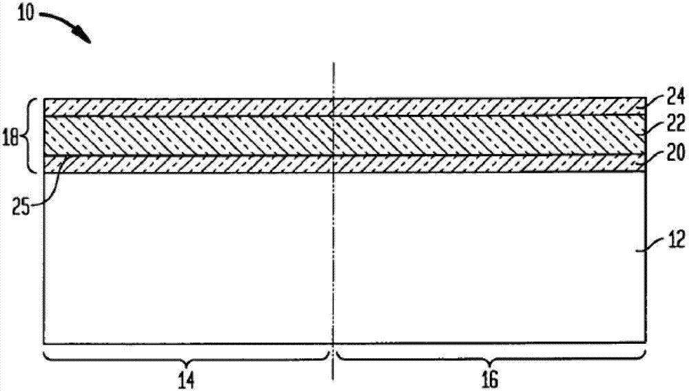
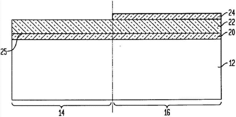
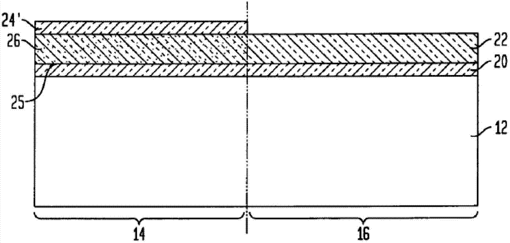
[0022] The first step is to provide an initial structure 10 comprising a semiconductor substrate 12 including at least one nFET device region 14 and at least one pFET device region 16 . Initial structure 10 also includes material stack 18 on top of substrate 12 in nFET device region 14 and pFET device region 16 . Material stack 18 includes, from bottom to top, gate dielectric 20 , first pol...


PUM


Abstract

The invention provides a method for improving polysilicon depletion of a double-gate CMOS (complementary metal oxide semiconductor) and the double-gate CMOS. The method comprises the following steps of: providing an initial structure, wherein the initial structure comprises a semiconductor substrate, the semiconductor substrate comprises an nFET (negative-channel field-effect transistor) device area and a pFET (positive-channel field-effect transistor) device area, and the initial structure further comprises a gate dielectric, a first material containing polysilicon and hard mask silicon nitride which are arranged from the bottom to the top at the top of the substrate in the nFET device area and the pFET device area; removing part of a hard mask on one of the nFET device area and the pFET device area; performing gas phase doping or plasma immersion ion implantation to perform doping in the area on which the part of the hard mask is removed; forming a dielectric layer on the surface of the area on which the part of the hard mask is removed; utilizing the selectivity of the silicon nitride and a dielectric to remove the other part of the hard mask; and taking the dielectric layer as the hard mask to perform the gas phase doping or the plasma immersion ion implantation with another conductivity so as to perform doping in the area on which the other part of the hard mask is removed.

Description

technical field [0001] The present invention relates to a semiconductor manufacturing process, and more particularly, the present invention relates to a method for improving polysilicon depletion in a double-gate CMOS (complementary metal oxide semiconductor), and the double-gate CMOS produced thereby. Background technique [0002] The depletion of charge carriers at or near the interface between the gate oxide and the polysilicon gate (poly depletion effect) has become a problem in CMOS devices, particularly pFET devices among them. Depletion results in a substantial increase in gate dielectric thickness, thereby negatively impacting device performance. The depletion effect becomes more and more important as the gate oxide thickness decreases. [0003] US patent application US20070238276 "ontrol of poly-Si depletion in CMOS via gas phase doping" proposes a fabrication method of a CMOS structure, wherein gas phase doping is employed to provide the dopant at the gate dielect...

Claims


Application Information

Patent Timeline
IPC IPC(8): H01L21/8238
Inventor 张雄
Owner SHANGHAI HUAHONG GRACE SEMICON MFG CORP
Features
  • R&D
  • Intellectual Property
  • Life Sciences
  • Materials
  • Tech Scout
  • Unparalleled Data Quality
  • Higher Quality Content
  • 60% Fewer Hallucinations
Learn More