OR logic circuit and chip

A logic circuit and chip technology, applied in the electronic field, can solve problems such as the size limitation of MOS tube storage devices, and achieve the effects of good scalability, performance, and long data retention time

Active Publication Date: 2013-01-23
PEKING UNIV
View PDF2 Cites 8 Cited by
  • Summary
  • Abstract
  • Description
  • Claims
  • Application Information

AI Technical Summary

Problems solved by technology

[0002] Or logic circuits are usually based on metal-oxide-semiconductor (MOS, Metal-Oxide-Semiconductor) tube storage devices. As the requirements for chip integration become higher and higher, or the size of logic circuits is also decreasing, but due to MOS Due to the limitation of the size of the storage device itself, the OR logic circuit in the prior art has the smallest size technology node

Method used


Image

  • OR logic circuit and chip
  • OR logic circuit and chip
  • OR logic circuit and chip

Examples


Embodiment Construction

[0024] The technical solutions in the embodiments of the present invention will be clearly and completely described below in conjunction with the accompanying drawings in the embodiments of the present invention. Obviously, the described embodiments are only some, not all, embodiments of the present invention. Based on the embodiments of the present invention, all other embodiments obtained by persons of ordinary skill in the art without creative efforts fall within the protection scope of the present invention.

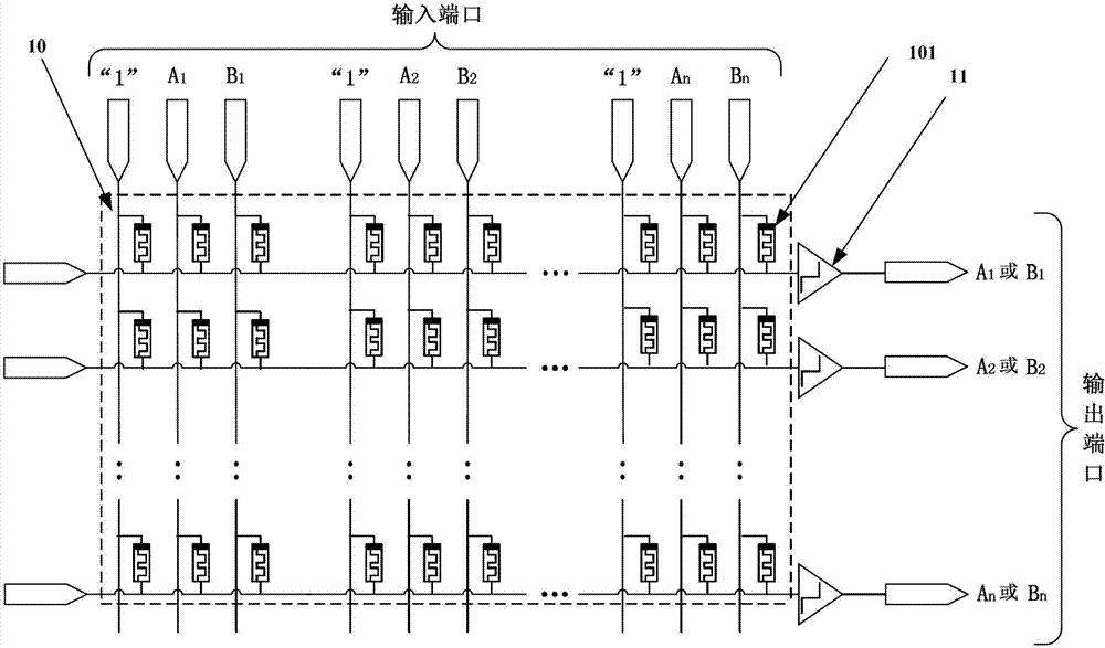
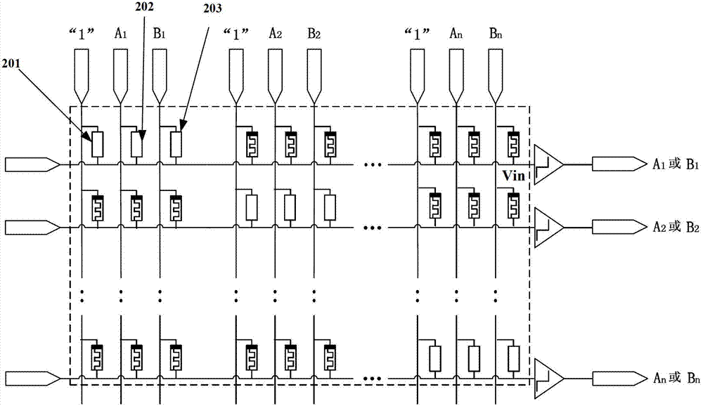
[0025] Such as figure 1 Shown is a schematic diagram of an OR logic circuit in an embodiment of the present invention.

[0026] The OR logic circuit may include a resistive memristor array 10 and a comparator 11 . In the resistive memristor array 10, the positive phase input terminals of the same column resistance variable memristor 101 are connected, so that the positive phase input terminal of the same column resistance variable memristor 101 is used as a signal i...


PUM


Abstract

The inventive embodiment discloses an OR logic circuit and a chip. The circuit comprises a resistance random memristor array and comparators, wherein the forward input ends of resistance random memristors on the same column in the resistance random memristor array are connected, so that the forward input ends of the resistance random memristors on the same column serves as a signal input end or an auxiliary signal input end of the OR logic circuit; the auxiliary signal input end is connected with a high level during work; the reverse input ends of the resistance random memristors on the same column in the resistance random memristor array are connected with the input end of one comparator, so that the output end of the comparator serves as a signal output end of the OR logic circuit; and the output end of the comparator outputs a high level or a low level when the voltage received by the input end of the comparator is larger or smaller than a threshold voltage. In the embodiment of the invention, the OR logic circuit can realize the programmable performance while saving the occupation area of the OR logic circuit.

Description

technical field [0001] The invention relates to the field of electronic technology, in particular to OR logic circuits and chips. Background technique [0002] Or logic circuits are usually based on metal-oxide-semiconductor (MOS, Metal-Oxide-Semiconductor) tube storage devices. As the requirements for chip integration become higher and higher, or the size of logic circuits is also decreasing, but due to MOS Due to the limitation of the size of the storage device itself, the OR logic circuit in the prior art has a minimum size technology node. Contents of the invention [0003] Embodiments of the present invention provide an OR logic circuit and a chip to solve the problem in the prior art that the OR logic circuit has a minimum size technology node. [0004] In order to solve the above problems, the embodiment of the present invention discloses the following technical solutions: [0005] On the one hand, an OR logic circuit is provided, including: an array of resistive ...

Claims


Application Information

Patent Timeline
Patent Type & Authority Applications(China)
IPC IPC(8): H03K19/20
Inventor 黄如张耀凯蔡一茂陈诚
Owner PEKING UNIV
Why Eureka
Try Eureka