Tunnel magnetic resistance device, and magnetic memory cell and magnetic random access memory using the same

a magnetic resistance device and tunnel magnetic technology, applied in solid-state devices, magnetic bodies, instruments, etc., can solve the problem of not being able to obtain the minimum necessary for a magnetic random access memory, or a magnetic memory cell, and achieve high thermal stability, long magnetic data retention time, and high thermal stability

Active Publication Date: 2011-02-22
TOHOKU UNIV
View PDF12 Cites 2 Cited by
  • Summary
  • Abstract
  • Description
  • Claims
  • Application Information

AI Technical Summary

Benefits of technology

[0011]The tunnel magnetic resistance device obtained according to an aspect of the present invention has a high thermal stability. A magnetic memory with such a tunnel magnetic resistance device becomes a nonvolatile memory with a high thermal stability, that is, with a long magnetic data retention time.

Problems solved by technology

As a result, the 200-mV read voltage, which is minimum necessary for a magnetic memory cell, or for a magnetic random access memory, cannot be obtained.

Method used


Image

  • Tunnel magnetic resistance device, and magnetic memory cell and magnetic random access memory using the same
  • Tunnel magnetic resistance device, and magnetic memory cell and magnetic random access memory using the same
  • Tunnel magnetic resistance device, and magnetic memory cell and magnetic random access memory using the same

Examples


example 1

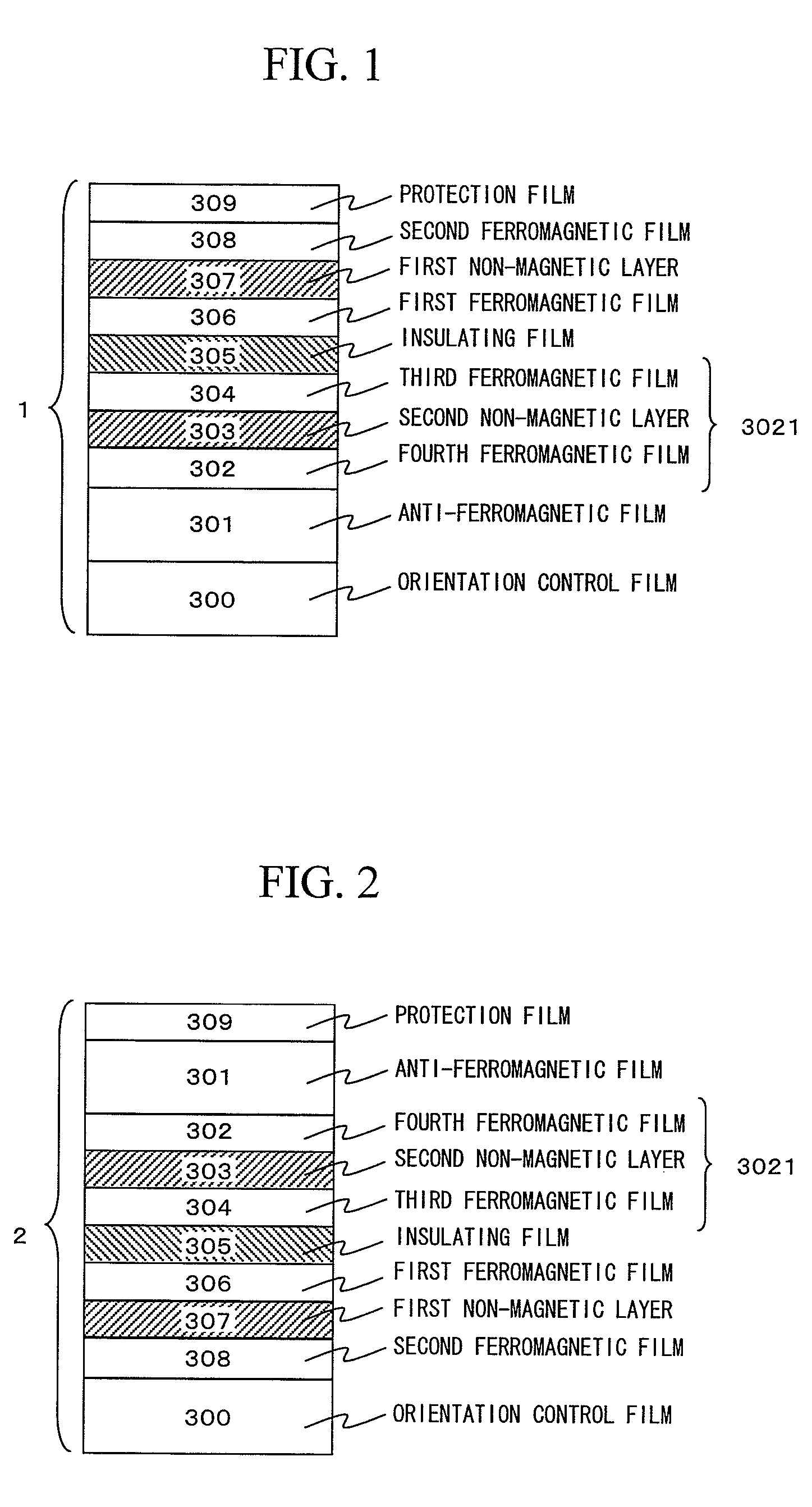
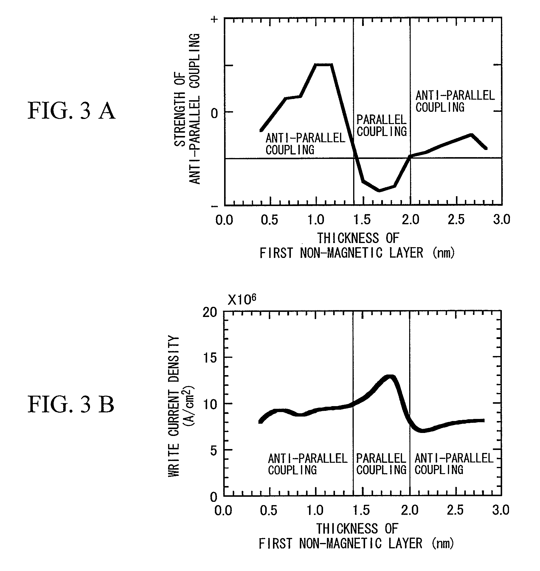
[0025]FIG. 1 is a schematic cross-sectional view of an example of a tunnel magnetic resistance device according to an aspect of the present invention. In this example, the tunnel magnetic resistance device was fabricated by a sputtering method. This tunnel magnetic resistance device 1 was made up of an orientation control film 300, an anti-ferromagnetic film 301, a ferromagnetic pinned layer 3021, an insulating film 305, a first ferromagnetic film 306, a first non-magnetic layer 307, a second ferromagnetic film 308, and a protection film 309. In the tunnel magnetic resistance device 1, the optimum magnetoresistance ratio was accomplished by a heat treatment under an appropriate temperature. A heat treatment at a temperature up to 400° C. can be carried out. The ferromagnetic pinned layer 3021 may, in some cases, include a fourth ferromagnetic film 302, a second non-magnetic layer 303, a third ferromagnetic film 304. In the descriptions that follow, the ferromagnetic pinned layer 302...

example 2

[0043]FIG. 2 is a schematic cross-sectional view of another example of a tunnel magnetic resistance device according to another aspect of the present invention. This tunnel magnetic resistance device 2 was made up of an orientation control film 300, a second ferromagnetic film 308, a first non-magnetic layer 307, a first ferromagnetic film 306, an insulating film 305, a ferromagnetic pinned layer 3021, an anti-ferromagnetic film 301, and a protection film 309. In a particular case where the first ferromagnetic film 306 and a third ferromagnetic film 304 were made of CoFeB, the crystal structure of each of these two films was a body center cubic lattice. The insulating film 305 was made of magnesium oxide crystal with a rock-salt structure, which was highly oriented in the (100) direction. The three layers—specifically, the first ferromagnetic film 306, the first non-magnetic layer 307 and the second ferromagnetic film 308—constitute the free layer of the tunnel magnetic resistance d...

example 3

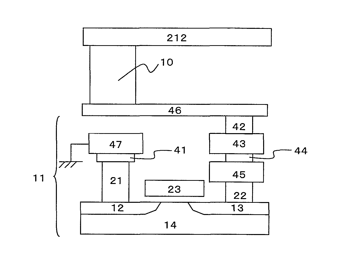
[0047]FIG. 10 is a schematic cross-sectional view showing a configuration example of a magnetic memory cell according to an aspect of the present invention. The magnetic memory cell includes a tunnel magnetic resistance device 10 as a memory cell, which is the same as ones shown in Examples 1 and 2.

[0048]A C-MOS 11 includes two n-type semiconductors 12 and 13 as well as a p-type semiconductor 14. An electrode 21 to be a drain electrode is electrically connected to the n-type semiconductor 12, and is connected, via an electrode 41 and an electrode 47, to the ground. An electrode 22 to be a source electrode is electrically connected to the n-type semiconductor 13. A gate electrode 23 is further provided. The ON / OFF of the current between the source electrode 22 and the drain electrode 21 is controlled by turning on / off the gate electrode 23. Layers of an electrode 45, an electrode 44, an electrode 43, an electrode 42 and an electrode 46 are formed on the source electrode 22. Via the a...


PUM


Abstract

Provided is a high-speed, super-low-power-consumption nonvolatile memory with a high thermal stability. A nonvolatile magnetic memory is equipped with high-output tunnel magnetic resistance devices to each of which a free layer with a high thermal stability is applied, while a writing method by spin transfer torque is applied to the memory. The tunnel magnetic resistance device has a free layer including a first ferromagnetic film and the second ferromagnetic film each of which has a body center cubic structure and each of which contains Co, Fe and B. The free layer, additionally, includes a first non-magnetic layer. The tunnel magnetic resistance device has a layered structure formed of the free layer and a pinned layer with a MgO insulating film with a (100) orientation rock-salt structure interposed in between.

Description

CLAIM OF PRIORITY[0001]The present application claims priority from Japanese application JP2006-122146 filed on Apr. 26, 2006, the content of which is hereby incorporated by reference into this application.BACKGROUND OF THE INVENTION[0002]1. Field of the Invention[0003]The present invention relates to a high-output tunnel magnetic resistance device with a high thermal stability, and to a low-power-consumption nonvolatile magnetic memory using the same.[0004]2. Description of the Related Art[0005]A tunnel magnetic resistance device using magnesium oxide as an insulating film disclosed in S. Yuasa. et al., Nature Material 3, 868 (2004), is a tunnel magnetic resistance device that is applied to a highly-integrated magnetic memory in the future, because, with the disclosed device, a magnetoresistance ratio that is several times larger than that with a tunnel magnetic resistance device using Al oxide as an insulator described in T. Miyazaki and N. Tezuka, J. Magn. Magn. Mater. 139, L231 ...

Claims


Application Information

Patent Timeline
Patent Type & Authority Patents(United States)
IPC IPC(8): G11C11/00
CPCB82Y25/00G11C11/16H01F10/3254H01L27/228H01L43/08H01F10/3272H10B61/22H10N50/10
Inventor HAYAKAWA, JUNOHNO, HIDEOIKEDA, SHOJILEE, YOUNG MIN
Owner TOHOKU UNIV
Why Eureka
Try Eureka