Memory Formed By Using Defects

a technology of defects and memory, applied in the field of memory, can solve the problems of source sb>1, source sb>1, and fbc memory device b>60/b> leakage current of floating-body capacitors, and achieve the effects of low power consumption, low cost and high density

Inactive Publication Date: 2011-02-10
NAT TAIWAN UNIV
View PDF1 Cites 2 Cited by
  • Summary
  • Abstract
  • Description
  • Claims
  • Application Information

AI Technical Summary

Benefits of technology

[0012]In accordance with one aspect of the present invention, a non-volatile memory formed by using channel defects in the channel is provided. The non-volatile memory has the advantages of low power consumption, low cost, high density and long data retention time.

Problems solved by technology

The disadvantage of using the floating gate 13 to trap the electric charges 15 is that once there are defects in the dielectric layer 12 around the floating gate 13, a part of the electric charges 15 will be lost.
The disadvantage of the FBC memory device 60 is the leakage current of the floating-body capacitor 48 and source S1.
Therefore, the FBC memory device 60 needs to be refreshed periodically, and thus the power consumption thereof is increased.

Method used


Image

  • Memory Formed By Using Defects
  • Memory Formed By Using Defects
  • Memory Formed By Using Defects

Examples


Embodiment Construction

[0050]The present invention will now be described more specifically with reference to the following embodiments. It is to be noted that the following descriptions of preferred embodiments of this invention are presented herein for the purposes of illustration and description only; it is not intended to be exhaustive or to be limited to the precise form disclosed.

[0051]The preferred embodiments of the present invention adopt the general n-type TFT semiconductor process, which only needs to use the polysilicon thin film transistor. Compared with the flash memory process, the present invention does not need extra expenditure of costs at all.

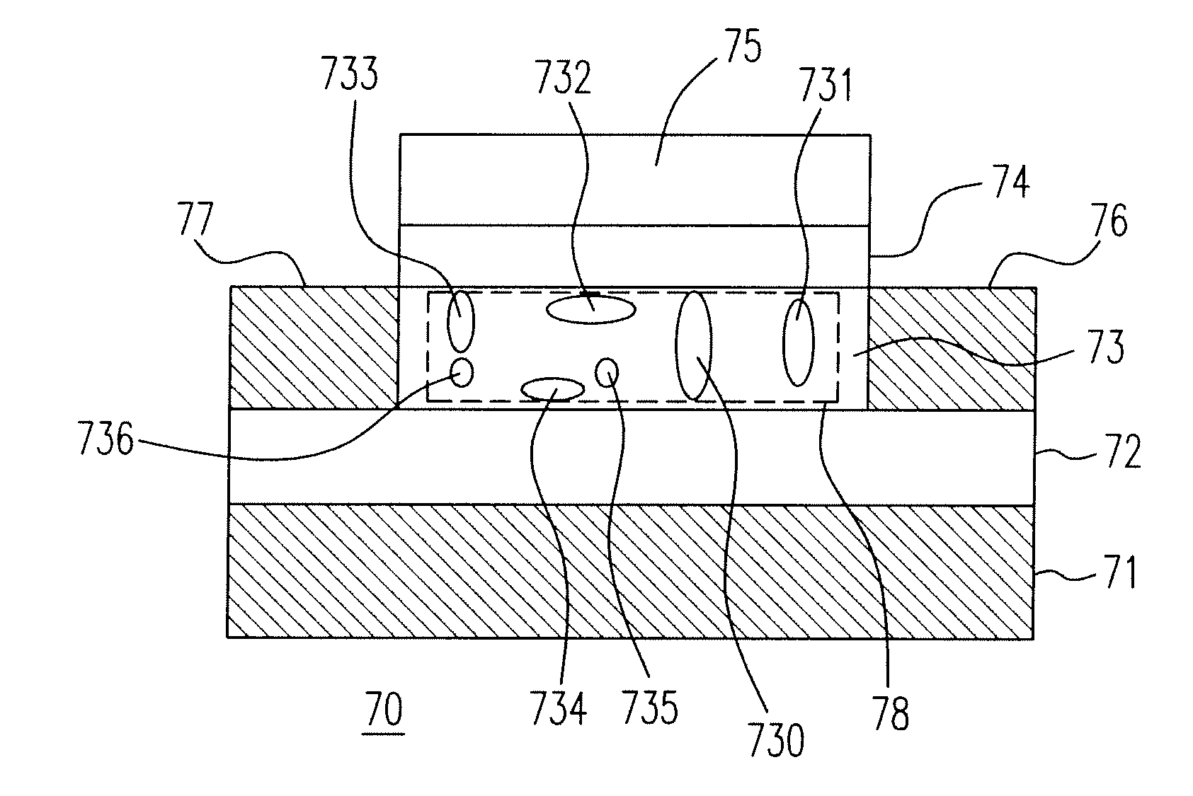
[0052]Please refer to FIG. 4(a), which shows the memory having defects according to a preferred embodiment of the present invention. The memory having defects 70 includes a second substrate 71, a first insulating layer 72, a p-type polysilicon active region 73, a gate insulating layer 74, a third gate 75, a second drain 76, a second source 77 and de...


PUM


Abstract

A non-volatile memory is provided. The non-volatile memory comprises at least a silicon-on-insulator transistor including a substrate; an insulating layer disposed on the substrate; an active region disposed on the insulating layer; and an energy barrier device disposed in the active region and outputting a relatively small current when the non-volatile memory is read.

Description

FIELD OF THE INVENTION[0001]The present invention relates to a memory, and more particularly to a non-volatile memory formed by using defects in a channel.BACKGROUND OF THE INVENTION[0002]With the diminution and diverse functions of the electronic product, the threshold voltage and current consumption of the memory therein are also getting lower. For a non-volatile memory, the material used and the storage method are both aiming at enhancing endurance times of reading, reducing the time of data writing / reading / erasing, prolonging the data retention time and reducing power consumption during operation.[0003]Please refer to FIG. 1(a), which shows a conventional EEPROM during writing. The EEPROM 10 has a logical state. For example, the structure of EEPROM 10 with a NMOS includes a p-type substrate 11, electric charges 15 and a gate 14. The p-type substrate 11 includes a source S and a drain D, and the gate 14 includes a dielectric layer 12 and a floating gate 13. During writing of the ...

Claims


Application Information

Patent Timeline
Patent Type & Authority Applications(United States)
IPC IPC(8): G11C16/04H01L21/66G11C11/34
CPCG11C16/02G11C16/0408H01L29/788H01L29/66825H01L29/685G11C2211/4016
Inventor CHEN, YEN-TINGHUANG, CHING-FANGSUN, HUNG-CHANGLIU, CHEE WEE
Owner NAT TAIWAN UNIV
Why Eureka
Try Eureka