Method for local high-doping and contacting of a semiconductor structure which comprises a solar cell or a precursor of a solar cell

A technology of solar cells and semiconductors, applied in semiconductor devices, semiconductor/solid-state device manufacturing, circuits, etc., can solve problems such as high cost and impracticality, and achieve the effects of improving light efficiency, reducing total contact resistance, and reducing surface recombination speed

Inactive Publication Date: 2013-01-23
FRAUNHOFER GESELLSCHAFT ZUR FOERDERUNG DER ANGEWANDTEN FORSCHUNG EV +1
View PDF6 Cites 5 Cited by
  • Summary
  • Abstract
  • Description
  • Claims
  • Application Information

AI Technical Summary

Problems solved by technology

This structure, which allows backside contacting for high efficiency, requires several additional photolithographic steps in fabrication besides the additional diffusion for highly doped regions, making industrial implementation of this solar cell structure impractical. or at least means very high cost

Method used


Image

  • Method for local high-doping and contacting of a semiconductor structure which comprises a solar cell or a precursor of a solar cell
  • Method for local high-doping and contacting of a semiconductor structure which comprises a solar cell or a precursor of a solar cell

Examples


Embodiment Construction

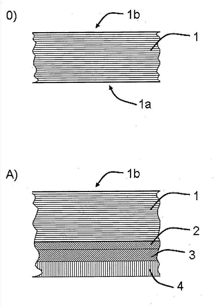
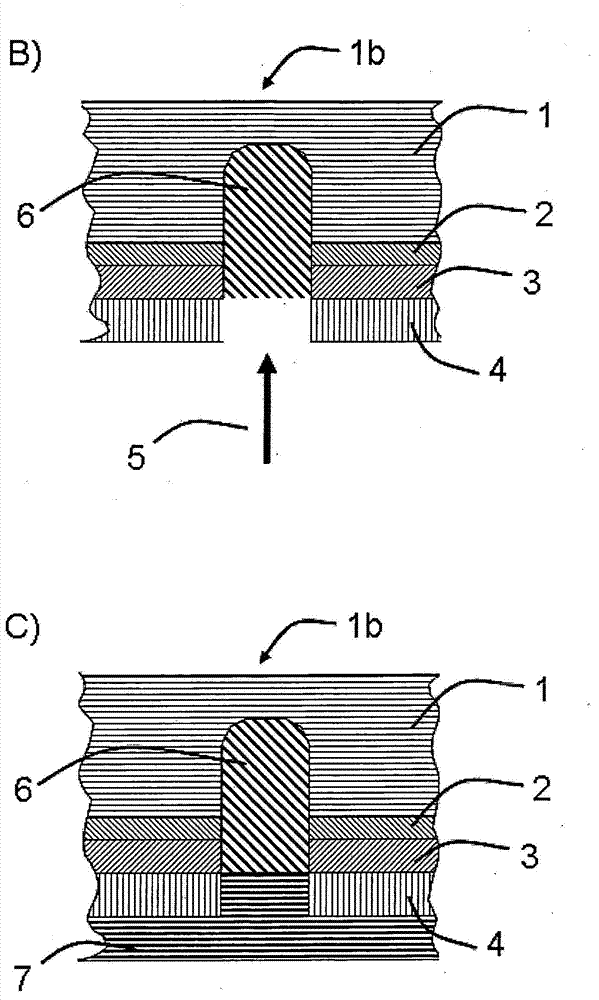
[0052] exist figure 1 and 2 An exemplary embodiment of the method according to the invention for locally highly doping and switching on a semiconductor structure which is a silicon solar cell precursor is shown in . The same reference numerals are used to denote the same elements throughout the drawings.

[0053] The semiconductor substrate 1 in the form of a silicon wafer has a uniform doping with a dopant concentration of 5×10 15 cm −3 . The solar cells to be produced are therefore n-type silicon solar cells.

[0054] In all the schematic diagrams shown in the figures, only a section of a semiconductor structure is shown, which respectively extends to the left and to the right. For better illustration, the diagrams are not shown to scale, especially with respect to the ratio of height and width.

[0055] The semiconductor substrate 1 has a contact surface 1 a, which is the rear side of the semiconductor substrate. In the completed solar cell, during operation, the semic...


PUM

PropertyMeasurementUnit
Thicknessaaaaaaaaaa
Thicknessaaaaaaaaaa
Thicknessaaaaaaaaaa

Abstract

The invention relates to a method for local high-doping and contacting of a semiconductor structure which is a solar cell or a precursor of a solar cell and has a silicon semiconductor substrate (1) of a base doping type. The high-doping and contacting is effected by producing a plurality of local high-doping regions of the base doping type in the semiconductor substrate (1) on a contacting side (1a) of the semiconductor substrate and applying a metal contacting layer (7) to the contacting side (1a) or, if applicable, one or more intermediate layers wholly or partially covering the contacting side (1a), to form electrically conductive connections between the metal contacting layer (7) and the semiconductor substrate (1) at the high doping regions.

Description

technical field [0001] The invention relates to a method according to the general concept of claim 1 for locally highly doped and switched-on semiconductor structures which are solar cells or solar cell precursors and which have a base doping type of silicon semiconductor substrate. Background technique [0002] In the case of photovoltaic solar cells based on silicon semiconductor substrates, numerous methods have been developed to achieve high efficiencies in the conversion of incident electromagnetic radiation into electrical energy on the one hand and cost-effective industrial production on the other hand. Especially in solar cells in which the emitter and the pn structure of the carrier pairs resulting from this separation are constructed on or in the front area of ​​the solar cell for light incidence, the electrical contacting of the base region is usually made by means of an arrangement on the rear side This is done by means of a metal connection layer which is elect...

Claims


Application Information

Patent Timeline
IPC IPC(8): H01L31/0216H01L31/0224H01L31/18H01L21/268H01L31/061
CPCH01L31/02168H01L31/061H01L31/022425H01L21/268H01L31/1804Y02E10/547Y02P70/50
Inventor 多米尼克·苏维托简·贝尼克乌尔里希·耶格尔
Owner FRAUNHOFER GESELLSCHAFT ZUR FOERDERUNG DER ANGEWANDTEN FORSCHUNG EV
Why Eureka
Try Eureka