
Method for manufacturing BJT (bipolar junction transistor) and BiCMOS (bipolar complementary metal oxide semiconductor)

A manufacturing method and transistor technology, applied in semiconductor/solid-state device manufacturing, electrical components, transistors, etc., can solve problems such as ineffective effects, serious surface recombination of emission regions, and influence on CMOS devices

Inactive Publication Date: 2013-02-06
CSMC TECH FAB1
View PDF3 Cites 5 Cited by
  • Summary
  • Abstract
  • Description
  • Claims
  • Application Information

AI Technical Summary

Problems solved by technology

[0006] 2. The emitter junction formed together with the implantation of the source and drain of the CMOS tube and its annealing is easily limited when adjusting the device parameters, and also affects the CMOS device;
[0007] 3. Direct chemical vapor deposition of polysilicon after dry etching SCl cleaning. Due to the relatively large ion damage during dry etching, the surface shape of the single crystal in the emission area is poor, the surface of the emission area is seriously recombined, and the small current amplification characteristics of BJT are relatively poor.
[0008] Therefore, the current polysilicon emitter process is relatively immature, the effect is not obvious, the process is unstable, and its maximum advantages cannot be fully utilized.

Method used


Image

  • Method for manufacturing BJT (bipolar junction transistor) and BiCMOS (bipolar complementary metal oxide semiconductor)
  • Method for manufacturing BJT (bipolar junction transistor) and BiCMOS (bipolar complementary metal oxide semiconductor)
  • Method for manufacturing BJT (bipolar junction transistor) and BiCMOS (bipolar complementary metal oxide semiconductor)

Examples


Embodiment Construction

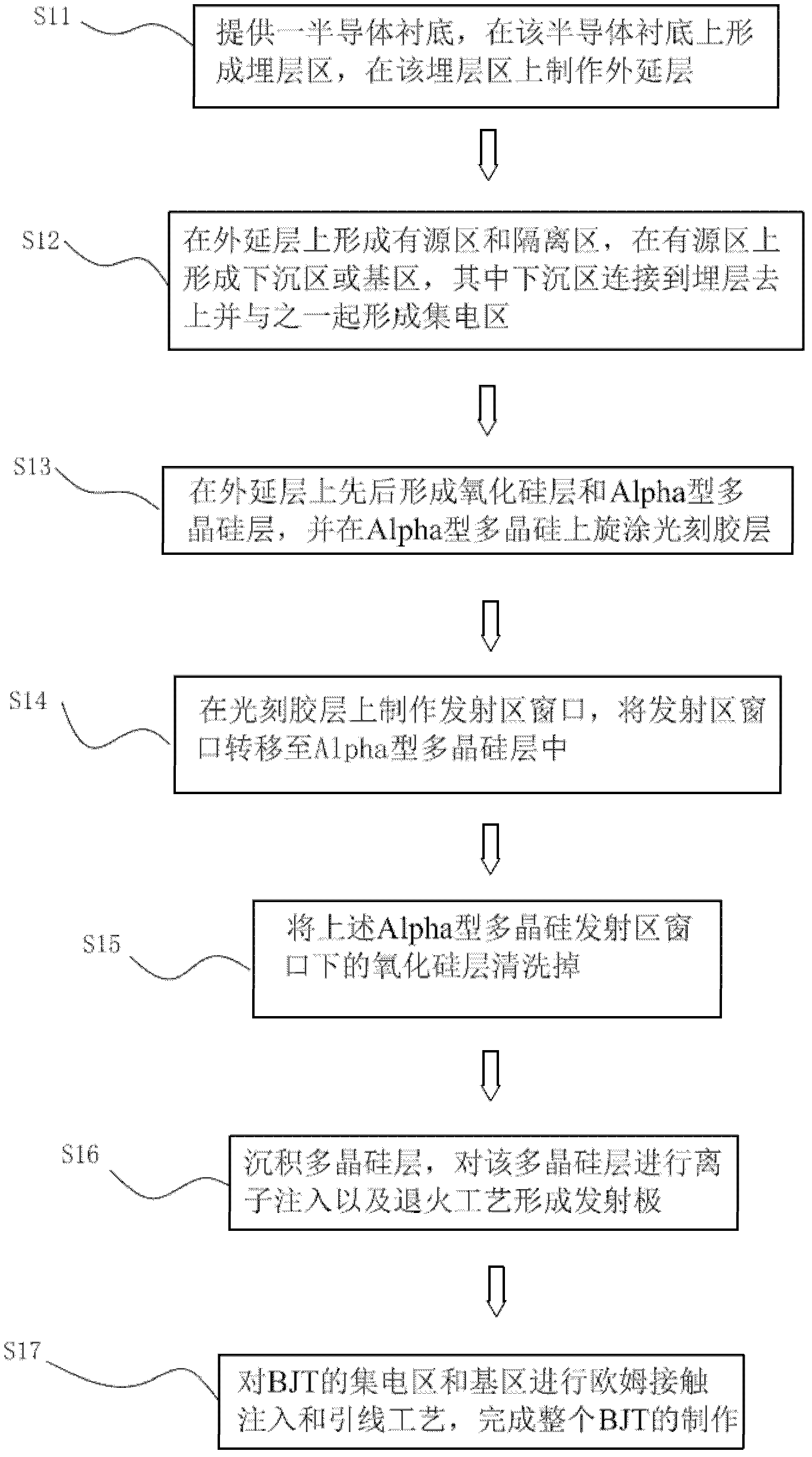
[0043]As introduced in the background technology, in the existing BiCMOS process, there are two main problems when making the emitter of the BJT: first, when the emitter window is formed by dry etching, due to the impact of etching ions on the single crystal silicon The damage on the surface is relatively large, which makes the surface shape of the single crystal silicon poor, and the phenomenon of recombination with the surface of polysilicon subsequently deposited on the single crystal silicon is serious, resulting in poor small current amplification characteristics of the BJT. Second, because in the existing process, the ion implantation process and annealing process of making the BJT emitter and the source and drain of the CMOS are carried out at the same time, so the junction depth formed by the emitter is relatively large and the ion concentration on the surface is also low. It will be very high, and it will also greatly limit the design flexibility of BJT and CMOS.

[0...


PUM

PropertyMeasurementUnit
Thicknessaaaaaaaaaa
Resistivityaaaaaaaaaa
Groove depthaaaaaaaaaa

Abstract

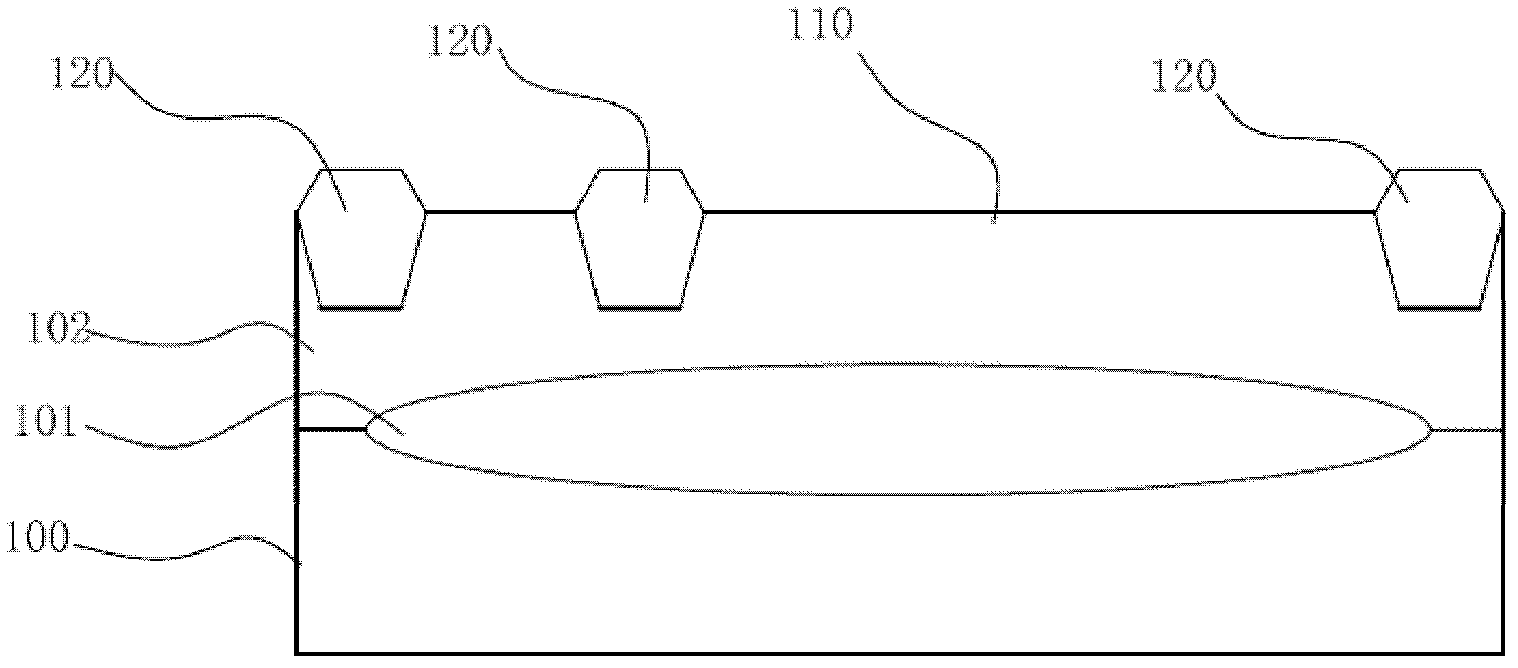
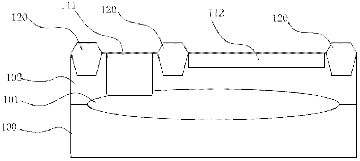
The invention discloses a method for manufacturing a BJT (bipolar junction transistor) and BiCMOS (bipolar complementary metal oxide semiconductor), wherein the BJT is provided with a polycrystalline silicon emitter, and the polycrystalline silicon emitter is manufactured by adopting the following two-step etching method: dry method etching is adopted in the first step, silicon dioxide is used as a retention layer, and the surface of monocrystalline silicon cannot be damaged; wet method etching is adopted in the second step, Alpha-type polycrystalline is used as a barrier layer, the crosswise corrosion volume to the silicon dioxide in the wet method etching is reduced, and a better window form is obtained. When an emitter region is used for polycrystalline ion injection and diffusion, better surface concentration can be obtained, and the low-current degradation of the BJT is improved.

Description

technical field [0001] The invention relates to a method for manufacturing a bipolar junction transistor and a bipolar-complementary metal oxide semiconductor hybrid structure, in particular to a bipolar junction transistor with a polysilicon emitter and a bipolar-complementary metal oxide semiconductor hybrid structure production method. Background technique [0002] Bipolar and complementary metal-oxide-semiconductor (BiCMOS) is an integrated circuit composed of a bipolar gate circuit and a complementary metal-oxide semiconductor (CMOS) gate circuit. The feature is that the bipolar (Bipolar) process is compatible with the CMOS process, and the bipolar circuit and the CMOS circuit are integrated in a certain circuit form on the same chip, and it has the characteristics of high density, low power consumption, and high-speed and large driving capability. . But the disadvantage is that its manufacturing process is also complicated, the cost is relatively high, and the device...

Claims


Application Information

Patent Timeline
IPC IPC(8): H01L21/8249H01L21/265
CPCH01L29/66272H01L27/0623H01L29/732H01L21/8249
Inventor 青云胡金节李月影胡勇海
Owner CSMC TECH FAB1
Learn More