

Isolation filling manufacture method in GaN-based high voltage light-emitting diode (LED) manufacture process
A technology of manufacturing process and manufacturing method, which is applied in semiconductor/solid-state device manufacturing, electrical components, circuits, etc., can solve the problems of insufficient etching depth, damage to the etching epitaxial layer, and high mask requirements, so as to reduce the difficulty and improve the Yield rate, the effect of improving coverage quality
- Summary
- Abstract
- Description
- Claims
- Application Information
AI Technical Summary
Problems solved by technology
Method used
Image

Examples
Embodiment Construction
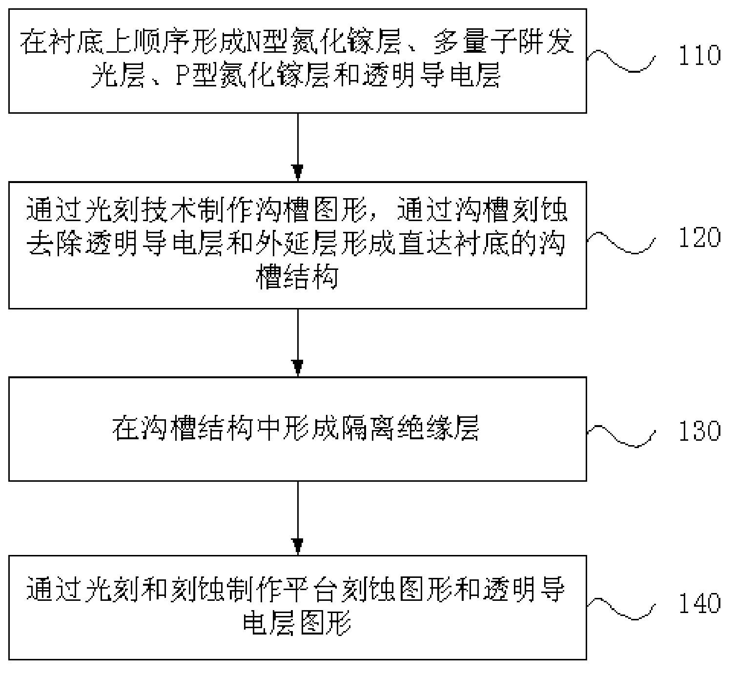
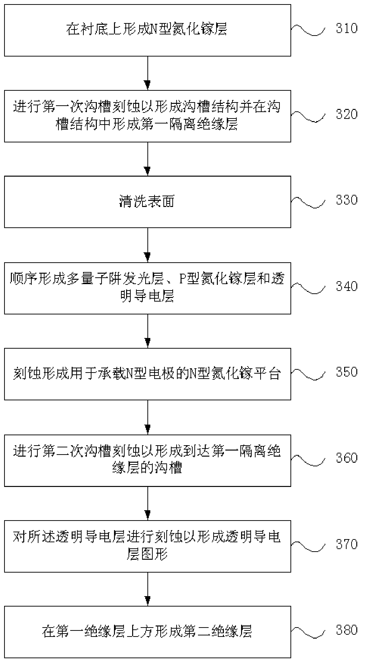
[0043] The technical solutions of the present invention will be further described below in conjunction with the accompanying drawings and through specific implementation methods. It should be understood that the specific embodiments described here are only used to explain the present invention, but not to limit the present invention. It should also be noted that, for ease of description, only steps related to the present invention are shown in the drawings but not all processes.
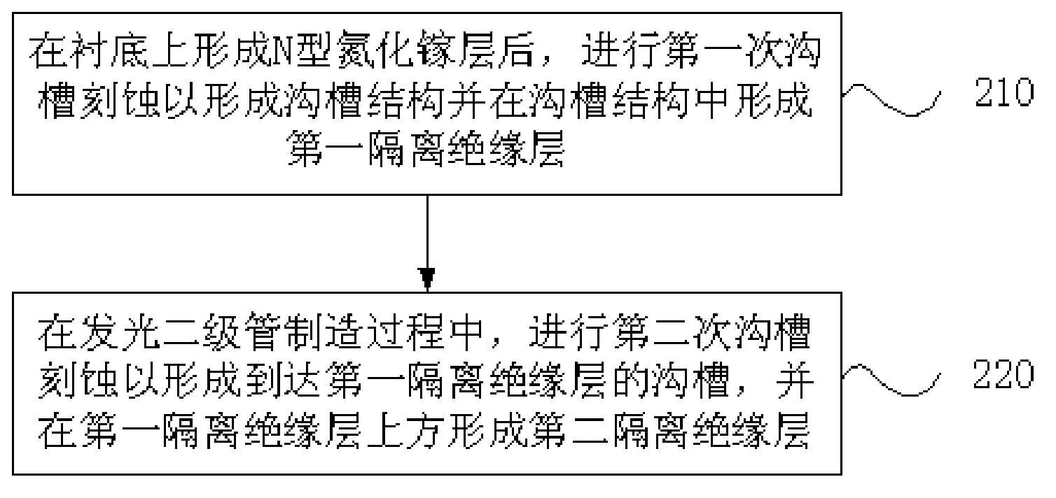
[0044] figure 2 It is a flow chart of the isolation filling manufacturing method in the GaN-based high-voltage light-emitting diode manufacturing process according to the embodiment of the present invention. Such as figure 2 As shown, the method includes:
[0045] Step 210, after forming the N-type gallium nitride layer on the substrate, performing the first trench etching to form a trench structure and forming a first isolation insulating layer in the trench structure;
[0046] Step 220 , duri...
PUM
 Abstract
Description
Claims
Application Information