LED (light-emitting diode) daylight lamp packaging module

A technology of LED fluorescent lamps and packaging modules, which is applied in the direction of electrical components, circuits, semiconductor devices, etc., can solve the problems of high loss of SMD packaged lamp beads, many patch welding processes, affecting light decay and life, etc., so as to reduce the quality. Stability, good energy saving and environmental protection benefits, and the effect of prolonging life

Inactive Publication Date: 2013-02-27
SHAOXING SHANGDING INTELLIGENT CONTROL ELECTRONICSCINECE & TECH
View PDF5 Cites 1 Cited by
  • Summary
  • Abstract
  • Description
  • Claims
  • Application Information

AI Technical Summary

Problems solved by technology

[0007] This kind of LED lamp technology and process structure has the following shortcomings: 1. There are many procedures and complex processes for patch welding; 2. Restricted by labor-intensive industries, the production efficiency is low; 3. Affected by manual welding, the process Rough, unstable quality; 4. SMD packaging lamp beads have a lot of loss; 5. Semiconductor chips are affected by high temperature and strong static electricity to affect light decay and life; 6. At the same time, small companies will over-rely on external processing manufacturers; 7. Manufacturers need to purchase more Equipment processing and more labor costs; 8. Production equipment needs to consume more resources

Method used


Image

  • LED (light-emitting diode) daylight lamp packaging module
  • LED (light-emitting diode) daylight lamp packaging module

Examples


Embodiment Construction

[0029] The present invention will be further described below in conjunction with the accompanying drawings and specific embodiments.

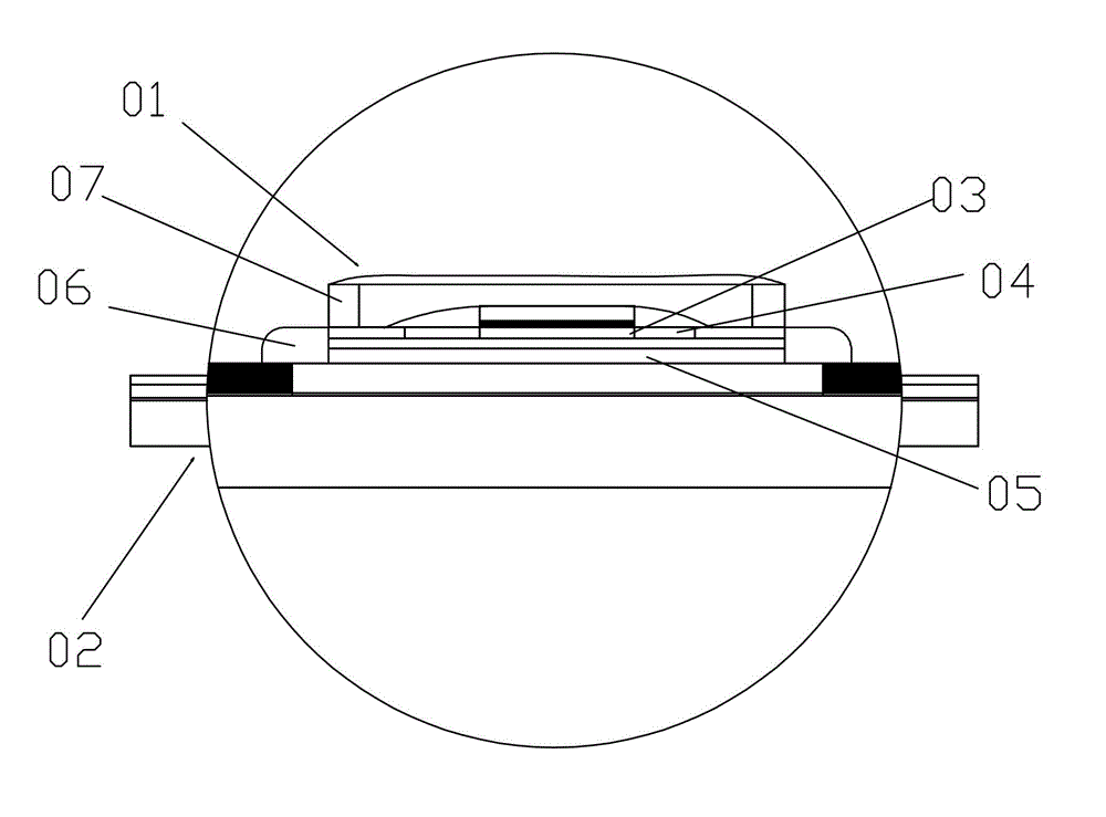
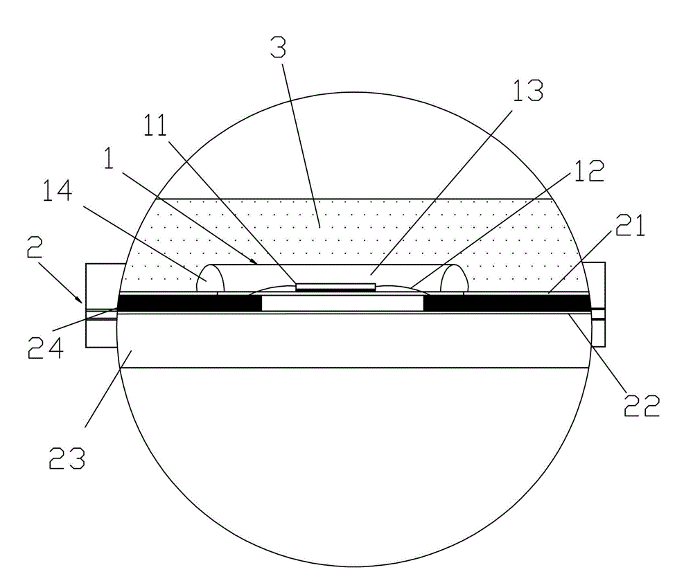
[0030] As shown in the figure, an LED fluorescent lamp packaging module disclosed by the present invention includes a lamp bead 1, a heat-conducting circuit board 2, and a lens 3. The lamp bead 1 includes a chip 11, and the upper layer of the chip 11 is coated with phosphor powder 13, and the chip 11 is passed through a solid state. The crystal glue is fixed on the thermally conductive circuit board 2 . The fluorescent powder 13 is surrounded by a white epoxy resin layer 14, and is cured and encapsulated by high temperature.

[0031] The outermost layer of the module is an optical lens 3 formed by a transparent resin silicone layer, which allows the light emitted by the semiconductor chip 11 to optically diffuse through the silicone lens 3, and also functions as a sealed module to achieve the highest IP protection level, protecting the packaged...


PUM


Abstract

The invention relates to the field of LEDs (light-emitting diode), and in particular relates to an LED (light-emitting diode) daylight lamp packaging module. The LED daylight lamp packaging module comprises a lamp bead, a heat conduction circuit board and a lens, wherein the lamp bead is directly packaged on the heat conduction circuit board through solid phase crystallization, and the lens is covered on the lamp bead and the heat conduction circuit board. By adopting the structure, the production efficiency and product quality of the LED daylight lamp are improved, the original delivery property of an LED chip is ensured, and the service life of an LED fluorescent tube is prolonged.

Description

[0001] technical field [0002] [0003] The invention relates to the field of LEDs, in particular to an LED fluorescent lamp packaging module. [0004] Background technique [0005] The internal structure of existing LED fluorescent lamps is mainly welded by various types of SMD packaged lamp beads and circuit substrates. Driven by a built-in power supply, input voltage and current, and connect the positive and negative electrical circuits of the substrate to make the packaged chip work and emit light. [0006] Its structure is as figure 1 As shown: between the lamp beads 01 and the heat-conducting circuit board 02, there are aluminum brackets 03, lead pins 04, solder paste 05, solder strips 06 and plastic molds 07 for fixing the lamp beads. [0007] This kind of LED lamp technology and process structure has the following shortcomings: 1. There are many procedures and complicated processes for patch welding; 2. Restricted by labor-intensive industries, the production...

Claims


Application Information

Patent Timeline
Patent Type & Authority Applications(China)
IPC IPC(8): H01L33/48H01L33/62
Inventor 沈国标
Owner SHAOXING SHANGDING INTELLIGENT CONTROL ELECTRONICSCINECE & TECH
Why Eureka
Try Eureka