Check patentability & draft patents in minutes with Patsnap Eureka AI!

Image enhancement processing system and method based on camera image processing chip

A technology of image enhancement and processing method, which is applied in the directions of image enhancement, image data processing, image data processing, etc., can solve problems such as unacceptable cost, and achieve the effect of reducing chip design cost, size, and chip area

Active Publication Date: 2013-03-06
ANYKA (GUANGZHOU) MICROELECTRONICS TECH CO LTD
View PDF6 Cites 15 Cited by
  • Summary
  • Abstract
  • Description
  • Claims
  • Application Information

AI Technical Summary

Problems solved by technology

[0005] Such memory overhead is acceptable for small-sized image processing chips, but for the current resolution of tens of millions, if each level of block processing needs to store block height + 1 line of data, then 3~ Level 4 processing chips require hundreds of kilobytes of cache memory. For low-level chips, the cost is unacceptable.

Method used


Image

  • Image enhancement processing system and method based on camera image processing chip
  • Image enhancement processing system and method based on camera image processing chip
  • Image enhancement processing system and method based on camera image processing chip

Examples


Embodiment Construction
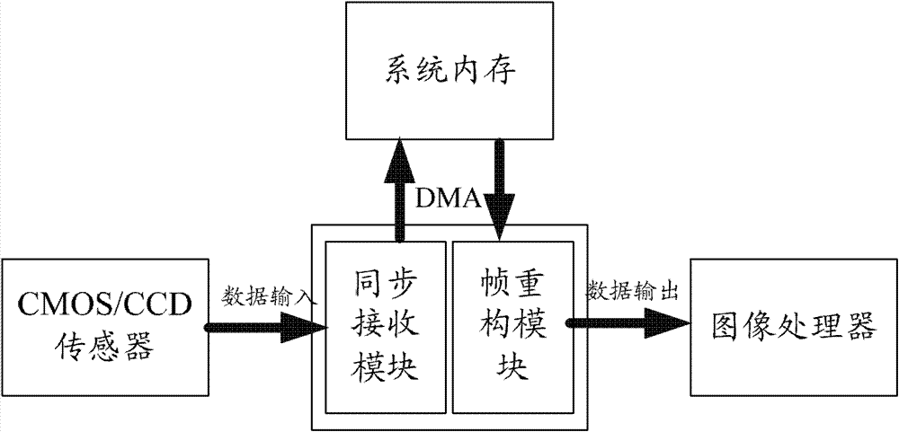
[0030] The core idea of ​​the present invention is that when processing large-scale images, a method of changing the chip area with time is used to perform virtual frame segmentation processing on the processed image at the source, and the interface to the subsequent stage remains unchanged. In the ISP image enhancement processing module, slightly modify the pre-stage acquisition and post-stage output part, and cooperate with the driver modification, to support larger image processing on the chip structure that supports the original small-size image.

[0031] In order to enable those skilled in the art to better understand the technical solutions of the present invention, the present invention will be further described in detail below in conjunction with the accompanying drawings and specific embodiments.

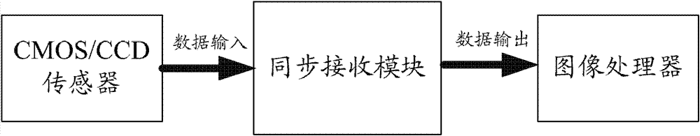
[0032] see image 3 , represents an embodiment of the image enhancement processing system based on the camera image signal processing chip of the present invention. It inc...


PUM


Abstract

The invention relates to the design field of chips and particularly discloses an image enhancement processing system and method based on a camera image processing chip. When a large-sized image is treated, image data is firstly uploaded to a system memory, then dividing along a line direction according to a back level processing capability and dividing a frame of large-sized image into a plurality of smaller images with equal height, wherein each line block is matched with synchronization signals so as to form isolated virtual frames; and then corresponding image enhancement treatment is implemented to each virtual frame. Trough the method for changing the chip area by time, the size of the module level cache can be greatly reduced, the chip area can be decreased and the design cost of the chip can be reduced.

Description

technical field [0001] The invention belongs to the field of chip design, and in particular relates to a control method, device and system for large-scale image processing, in particular to an image enhancement processing system and processing method based on a camera image processing chip. Background technique [0002] The data transmission format of mainstream CMOS / CCD image sensors (sensors) when collecting large-scale images is generally Bayer Raw RGB format, such as figure 1 As shown, the characteristic of this data format is that a pixel has only one color component (R, G or B) information, and then a complete RGB pixel is obtained through an algorithm such as interpolation; at the same time, some images will be introduced during the acquisition process. Noise, including dead pixels of the lens, etc. In the camera image signal processing chip ISP (image signal processor), it is necessary to enhance the original collected image. The system structure is as follows: fi...

Claims


Application Information

Patent Timeline
IPC IPC(8): G06T1/00G06T5/00
Inventor 蔡宁宁刘济凌胡胜发
Owner ANYKA (GUANGZHOU) MICROELECTRONICS TECH CO LTD
Features
  • R&D
  • Intellectual Property
  • Life Sciences
  • Materials
  • Tech Scout
  • Unparalleled Data Quality
  • Higher Quality Content
  • 60% Fewer Hallucinations
Learn More