Display apparatus and image pickup apparatus
A technology for display devices and light-emitting layers, which can be used in the manufacture of electrical components, electrical solid-state devices, semiconductor/solid-state devices, etc., and can solve problems such as difficulties in preparing and maintaining metal masks.
- Summary
- Abstract
- Description
- Claims
- Application Information
AI Technical Summary
Problems solved by technology
Method used
Image
Examples
Embodiment 1
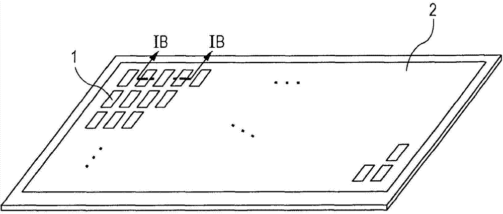
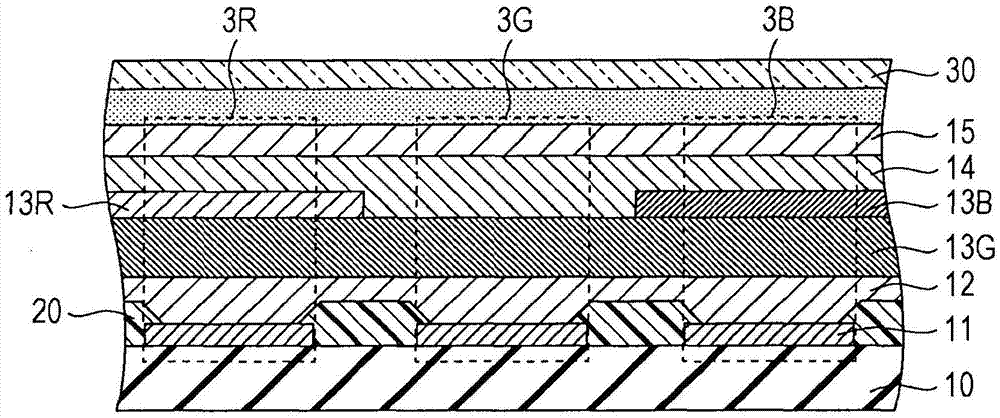
[0073] prepared with Figure 1A and 1B A display device of the configuration shown in . This example corresponds to the first embodiment. This embodiment is a bottom emission type display device in which light is extracted from the surface on the substrate 10 side.
[0074] A low-temperature polysilicon thin film transistor (TFT) is formed on a glass substrate, and an interlayer insulating film made of silicon nitride and a planarizing film made of acrylic resin are formed thereon, so that the fabrication Figure 1A Substrate 10 shown in . An ITO film having a thickness of 100 nm was formed on the substrate 10 by a sputtering method. Subsequently, the ITO film was patterned on a pixel basis to form the anode 11 .
[0075] An acrylic resin was formed on the anode 11 by spin coating, and the acrylic resin was patterned by lithography to form the insulating layer 20 . Clean ultrasonically with isopropyl alcohol (IPA) and by boiling, then dry. Furthermore, after UV / ozone clea...
Embodiment 2
[0107] Preparation settings have image 3 A display device of an organic electroluminescent element having the structure shown in . This example corresponds to the second embodiment. This embodiment is a top emission type organic electroluminescence element in which light is extracted from the opposite surface of the substrate 10 .
[0108] This embodiment differs from Embodiment 1 in the configuration of the anode 11 and the cathode 15, the configuration and formation order of the blue light emitting layer 13B, and the configuration of the electron injection layer. Only the parts different from Embodiment 1 will be described below.
[0109] The anode 11 is formed of an aluminum alloy and an ITO film. Specifically, in formation, a film of an aluminum alloy having a thickness of 200 nm was formed as a reflective electrode, an ITO film was formed having a thickness of 20 nm, and the aluminum alloy and the ITO film were patterned on a pixel basis.
[0110] In this embodiment,...
PUM
 Abstract
Description
Claims
Application Information


