Manufacturing method of top-gate oxide thin-film transistor

A technology of oxide film and manufacturing method, which is applied in semiconductor/solid-state device manufacturing, electrical components, circuits, etc.

Active Publication Date: 2013-03-27
SHENZHEN DANBANG INVESTMENT GROUP
View PDF6 Cites 17 Cited by
  • Summary
  • Abstract
  • Description
  • Claims
  • Application Information

AI Technical Summary

Problems solved by technology

[0005] In order to solve the above technical problems, so that the field effect mobility of the transistor is higher, and the current crowding phenomenon is not easy

Method used


Image

  • Manufacturing method of top-gate oxide thin-film transistor
  • Manufacturing method of top-gate oxide thin-film transistor

Examples


Embodiment 1

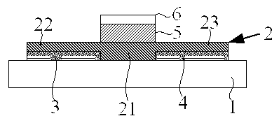
[0040] like figure 1 As shown, a top gate oxide thin film transistor of an embodiment includes a substrate 1, a source 3 and a drain 4 formed on the substrate 1, an oxide semiconductor formed on the source 3, the drain 4 and the substrate 1 layer 2, a gate insulating layer 5 on the oxide semiconductor layer 2, and a gate 5 on the gate insulating layer 5, the oxide semiconductor layer 2 includes a channel region 21 corresponding to the gate region, and a channel A region 22 and a region 23 on both sides of the region 21 are respectively in contact with the source 3 and the drain 4, and the channel region 21 is located between the source 3 and the drain 4, wherein the gate 6 and the insulating layer 5 and the channel region 21 can be form self-alignment.

[0041] The manufacturing method of the top gate oxide thin film transistor of this embodiment includes the following steps:

[0042] 1.1. The substrate 1 can be glass, quartz, silicon wafer or other flexible substrates such ...

Embodiment 2

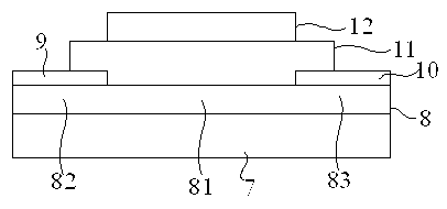
[0053] like figure 2 As shown, the top gate oxide thin film transistor includes a substrate 7, an oxide semiconductor layer 8 formed on the substrate 7, a source 9 and a drain 10 formed on the oxide semiconductor layer 8, a source 3 and a drain formed on the 4 and the gate insulating layer 11 on the oxide semiconductor layer 8, and the gate 12 formed on the gate insulating layer 11. The oxide semiconductor layer 8 includes a channel region 81 corresponding to the gate region, and the two sides of the channel are respectively contacted. To the regions 82 and 83 of the source and drain electrodes 9 and 10, the channel region is located between the source 9 and the drain 10;

[0054] The manufacturing method of the top gate oxide thin film transistor of this embodiment includes the following steps:

[0055] 2.1. The substrate 7 can be glass, quartz, silicon wafer or other flexible substrates such as plastic, stainless steel, etc., and an oxide semiconductor film is deposited on...


PUM

PropertyMeasurementUnit
Thicknessaaaaaaaaaa
Carrier concentrationaaaaaaaaaa
Thicknessaaaaaaaaaa

Abstract

The invention discloses a manufacturing method of a top-gate oxide thin-film transistor. The top-gate oxide thin-film transistor comprises an oxide semiconductor layer, a source electrode and a drain electrode, the source electrode and the drain electrode respectively contact with the oxide semiconductor layer, and the oxide semiconductor layer is made of indium oxide, gallium oxide, zinc oxide or stannic oxide or binary or multibasic oxide of indium, gallium, zinc and stannum. The source electrode, the drain electrode and the oxide semiconductor layer are radiated by a variable magnetic field. Field effect migration rate of the top-gate thin-film transistor is high, and current crowding of the output characteristics is avoided when the drain electrode is at low voltage.

Description

technical field [0001] The invention relates to the field of top-gate thin film transistors, in particular to a method for manufacturing a top-gate oxide thin film transistor. Background technique [0002] Compared with the amorphous silicon TFT (thin film field effect transistor) widely used in the active drive matrix of liquid crystal display, the oxide semiconductor TFT has the following advantages: (1) high field effect mobility; (2) high switching ratio; (3) The temperature of the preparation process is low; (4) Large-area amorphous films can be produced, with good uniformity and good and consistent electrical properties; (5) Less affected by visible light, more stable than amorphous silicon and organic thin film transistors; (6) ) can be made into transparent devices. In the field of flat panel display, oxide TFT technology almost meets all the requirements of many display modes including AMOLED drive, fast ultra-large-screen liquid crystal display, 3D display and so ...

Claims


Application Information

Patent Timeline
IPC IPC(8): H01L21/336
Inventor 刘萍
Owner SHENZHEN DANBANG INVESTMENT GROUP
Why Eureka
Try Eureka