Method for preparing aluminum nanostructure array, three-dimensional solar cell and photovoltaic cell

A technology of solar cells and nanostructures, applied in electroforming nanostructures, photovoltaic power generation, circuits, etc., can solve the problems of high cost, controllability, poor scale, and high cost

Active Publication Date: 2013-03-27
THE HONG KONG UNIV OF SCI & TECH
View PDF5 Cites 12 Cited by
  • Summary
  • Abstract
  • Description
  • Claims
  • Application Information

AI Technical Summary

Problems solved by technology

Although 3D nanostructured materials have proven to be very effective in promoting broadband absorption and light trapping, these top-down and bottom-up approaches are still expensive, complex, controllable, and poorly scalable
If 3D nanostructured materials are used as anti-reflection coatings or anti-reflection templates for solar cells, the disadvantages of these top-down and bottom-up methods, such as high cost, complexity, controllability, and poor scale, will limit the development of 3D nanostructures. Applications of Structural Materials
[0006] The background mentioned above is only an overview of the synthesis of three-dimensional nanostructured materials and their application in anti-reflection coatings, and is not thorough.

Method used


Image

  • Method for preparing aluminum nanostructure array, three-dimensional solar cell and photovoltaic cell
  • Method for preparing aluminum nanostructure array, three-dimensional solar cell and photovoltaic cell
  • Method for preparing aluminum nanostructure array, three-dimensional solar cell and photovoltaic cell

Examples


Embodiment Construction

[0044] Various aspects or features in the patent are described according to the drawings, and the same reference numerals in the specification are used to refer to the same elements. In this manual, in order to help better understand the manual, a large number of special details will be explained clearly. However, it should be understood that some aspects of the specification will not mention these details, or will be replaced by other methods, components, molecules, etc. In addition, in various embodiments, well-known structures and devices will be represented by block diagrams to help description and explanation.

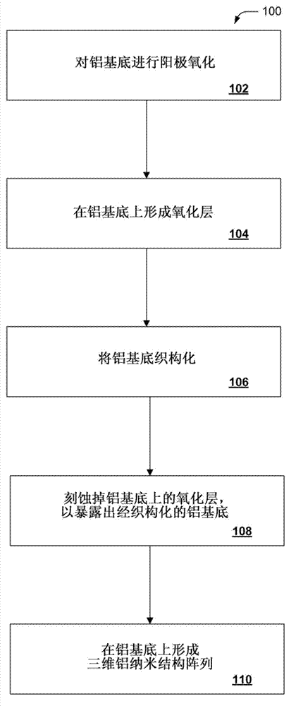
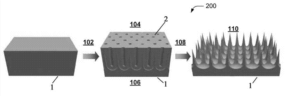
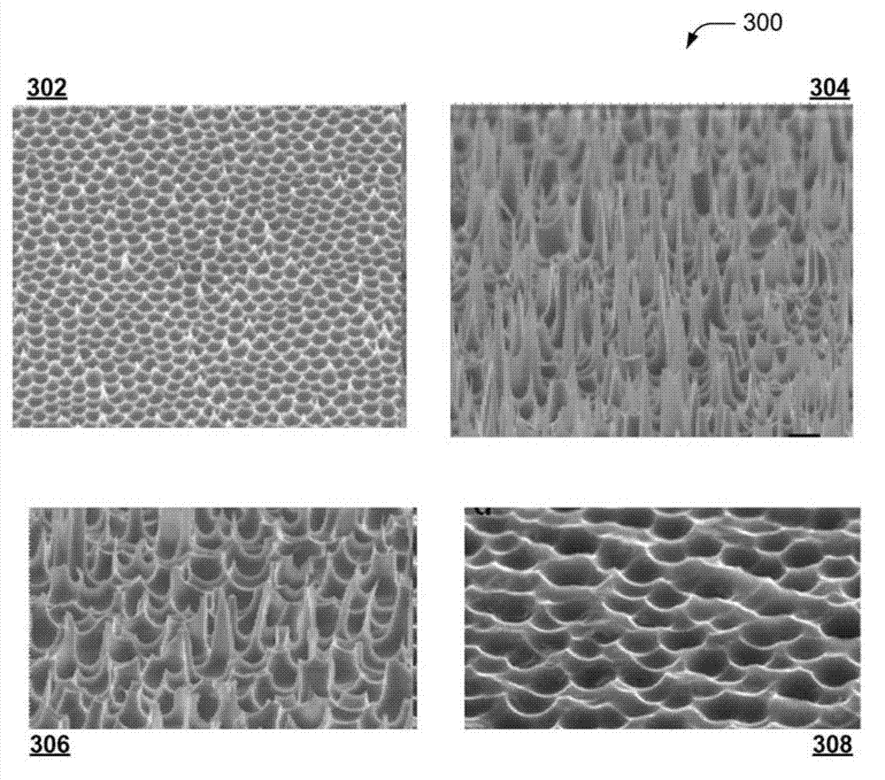
[0045] According to one or more embodiments described in this specification, a three-dimensional nanostructure array self-assembled and grown on an aluminum surface according to a low-cost and large-scale method is described here. After being coated with a light-absorbing film material, the three-dimensional nanostructure array exhibits a more effective light-absorb...


PUM

PropertyMeasurementUnit
diameteraaaaaaaaaa
heightaaaaaaaaaa
thicknessaaaaaaaaaa

Abstract

Described herein are a method for obtaining a three-dimensional nanostructure array on an aluminum substrate, a three-dimensional solar cell including such a three-dimensional nanostructure array, and a photovoltaic cell. The method includes anodizing the aluminum substrate; forming an oxide layer on the aluminum substrate; texturizing the aluminum substrate; etching the oxide layer from the aluminum substrate to expose the texturized aluminum substrate; and forming a three-dimensional aluminum nanostructure array on the aluminum substrate. The method is a low cost and scalable process to obtain three-dimensional nanostructure arrays on an aluminum surface. The three-dimensional nanostructure array, coated with a light absorber, is utilized in a thin film solar cell or photovoltaic cell. The reflectance of the solar cell and photovoltaic cell is low compared to the reflectance exhibited by the light absorber coated on a planar aluminum substrate.

Description

[0001] Related application [0002] This application claims priority to the U.S. Provisional Application 61 / 573,153 entitled "Self-assembled three-dimensional aluminum nano-nail array and its application in the field of effective light absorption and photovoltaic cells" filed on September 16, 2011. Technical field [0003] The present invention generally relates to a preparation method and application of a three-dimensional aluminum nanostructure array. Background technique [0004] Nanostructured materials have broad application prospects in anti-reflection coatings and solar cells. Three-dimensional nanostructured materials, such as nanotubes, nanorods, nanopillars, nanocones, nanodomes, and nanowires, are very attractive in anti-reflective coatings due to their large surface area. Compared with the surface structure of the two-dimensional textured substrate, the larger surface area of ​​the three-dimensional nanostructured material can promote broadband and more effective light ...

Claims


Application Information

Patent Timeline
Patent Type & Authority Applications(China)
IPC IPC(8): H01L31/18H01L31/20H01L31/0216
CPCC25D1/006H01L31/18C25D11/045H01L31/0236H01L31/02366Y02E10/50H01L31/0392H01L31/03926
Inventor 范智勇于睿
Owner THE HONG KONG UNIV OF SCI & TECH
Why Eureka
Try Eureka