Method for preventing over etching of passivation layers

A passivation layer and over-etching technology, which is applied in the manufacture of electrical components, circuits, semiconductors/solid-state devices, etc., can solve problems such as inconvenience, SiC over-etching, and inability to judge, so as to ensure the quality of etching and avoid over-etching Eclipse effect

Active Publication Date: 2013-04-03
INST OF MICROELECTRONICS CHINESE ACAD OF SCI
View PDF3 Cites 8 Cited by
  • Summary
  • Abstract
  • Description
  • Claims
  • Application Information

AI Technical Summary

Problems solved by technology

In this way, it is impossible to judge whether SiO is etched by detecting the etching rate during the etching process. 2 The interface with SiC is prone to over-etching of SiC
[0004] This shows, above-mentioned existing SiO on SiC Passivation layer etching, obviously still have inconvenience and defective, and urgently need to be further improved

Method used


Image

  • Method for preventing over etching of passivation layers
  • Method for preventing over etching of passivation layers
  • Method for preventing over etching of passivation layers

Examples


Embodiment Construction

[0024] In order to make the object, technical solution and advantages of the present invention clearer, the present invention will be described in further detail below in conjunction with specific embodiments and with reference to the accompanying drawings. Furthermore, while illustrations of parameters comprising particular values ​​may be provided herein, it should be understood that the parameters need not be exactly equal to the respective values, but rather can be approximated within acceptable error margins or design constraints.

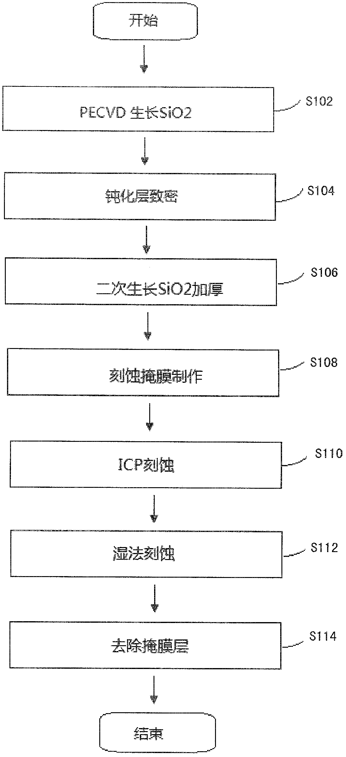
[0025] In an exemplary embodiment of the present invention, a method for preventing over-etching of a passivation layer is disclosed. The method includes:

[0026] In the passivation layer preparation stage:

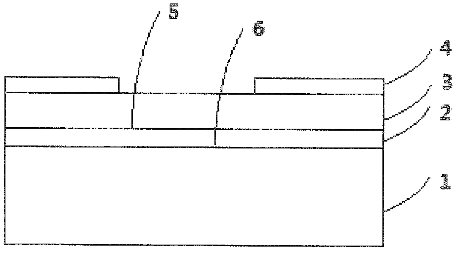
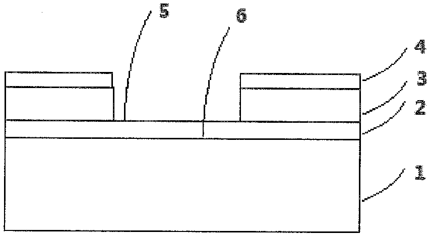
[0027] Step A, preparing two passivation layers with different densities on the substrate, the passivation layer close to the substrate side is a dense passivation layer, and the passivation layer far away from the substrate side is a l...


PUM

PropertyMeasurementUnit
Thicknessaaaaaaaaaa
Thicknessaaaaaaaaaa
Thicknessaaaaaaaaaa

Abstract

The invention discloses a method for preventing over etching of passivation layers, comprising the following steps of: step A, preparing two passivation layers different in compactness on a substrate, wherein the passivation layer close to the side of the substrate is a compact passivation layer, while the passivation layer far away from the side of the substrate is a loose passivation layer; step B, applying a photoresist on the passivation layers through spin coating, and exposing and developing the photoresist according to a predetermined element template; step C, with the photoresist left after exposure and development on the substrate as the mask, performing dry etching on the loose passivation layer; and step D, with the photoresist left after exposure and development on the substrate as the mask, performing wet etching on the compact passivation layer. The method provided by the invention avoids over etching of the base layer SiC and also guarantees the etching quality by growing two SiO2 layers different in compactness and separately etching the two SiO2 layers different in compactness by combining the advantages of the wet etching and the dry etching.

Description

technical field [0001] The invention relates to the field of component preparation technology in the microelectronics industry, in particular to a method for preventing overetching of a passivation layer. Background technique [0002] As a new generation of wide bandgap semiconductor material, silicon carbide (SiC) has attracted more and more attention. It has the characteristics of large bandgap width, high critical breakdown field strength, high electron mobility, and high thermal conductivity. Widespread concern. At present, SiC-based Schottky barrier diode (JBS) devices have been widely used in the field of power electronics. SiO in SiC JBS devices 2 The passivation layer can reduce the injection damage, protect the surface of the chip from contamination, and play the role of a thick passivation medium in the field plate. [0003] At present, the etching process of the passivation layer mainly includes dry etching and wet etching. For wet etching, it has strong etchi...

Claims


Application Information

Patent Timeline
IPC IPC(8): H01L21/311
Inventor 李博申华军白云汤益丹刘焕明周静涛杨成樾刘新宇
Owner INST OF MICROELECTRONICS CHINESE ACAD OF SCI
Why Eureka
Try Eureka