Patterned substrate and preparation method thereof

A graphics substrate and graphics technology, applied in the direction of electrical components, circuits, semiconductor devices, etc., to achieve the effect of improving light extraction efficiency and reducing multiple reflections

Active Publication Date: 2013-04-03
SHANDONG NOVOSHINE OPTOELECTRONICS CO LTD
View PDF7 Cites 11 Cited by
  • Summary
  • Abstract
  • Description
  • Claims
  • Application Information

AI Technical Summary

Problems solved by technology

Although there are many types of graphics in the existing patterned substrates, they are basically single-level patterned substrates using the same material.

Method used


Image

  • Patterned substrate and preparation method thereof
  • Patterned substrate and preparation method thereof
  • Patterned substrate and preparation method thereof

Examples


Embodiment 1

[0034] Embodiment 1: the preparation method of described figure substrate, adopt following process step:

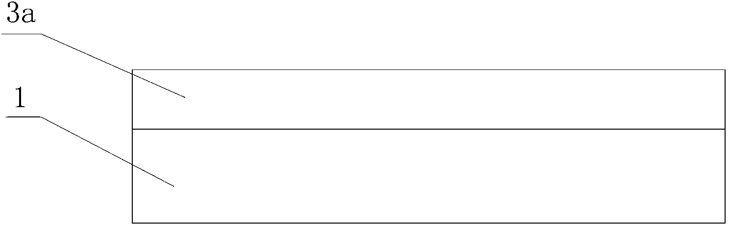
[0035] (1) Provide a basic substrate 1 with a front side and a back side, and the basic substrate 1 is a sapphire substrate; for example image 3 As shown, a layer of heterogeneous substrate 3a is formed on the upper surface of the basic substrate 1 to obtain a composite substrate. The thickness of the heterogeneous substrate 3a is 0.5 μm, and the material of the heterogeneous substrate 3a is SiO 2 、Si 3 N 4 , ZnO 2 , Si or GaAs;

[0036] (2) Clean the composite substrate;

[0037] (3) if Figure 4 As shown, a photoresist 4a is coated on the surface of the conductive substrate 3a of the composite substrate, and the thickness of the coating is 0.5 μm, and the exposure and development are carried out to expose the area to be etched;

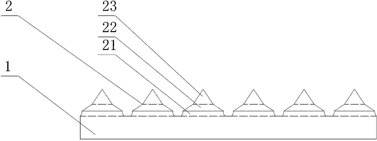
[0038] (4) Dry etching and wet etching are used to etch once respectively, the total etching depth is 1 μm, and pattern protrusions 2 a...

Embodiment 2

[0040] Embodiment 2: The preparation method of described graphics substrate adopts the following process steps:

[0041] (1) Provide a basic substrate 1 with a front side and a back side, and the basic substrate 1 is a silicon carbide substrate; for example image 3 As shown, a layer of heterogeneous substrate 3a is formed on the upper surface of the basic substrate 1 to obtain a composite substrate. The thickness of the heterogeneous substrate 3a is 2 μm, and the material of the heterogeneous substrate 3a is SiO 2 、Si 3 N 4 , ZnO 2 , Si or GaAs;

[0042] (2) Clean the composite substrate;

[0043] (3) if Figure 4 As shown, a photoresist 4a is coated on the surface of the conductive substrate 3a of the composite substrate, and the thickness of the coating is 4 μm, and the exposure and development are carried out to expose the area to be etched;

[0044] (4) Dry etching and wet etching are used to etch once respectively, the total etching depth is 4 μm, and pattern protrus...

Embodiment 3

[0046] Embodiment three: the preparation method of described graphics substrate adopts the following process steps:

[0047] (1) Provide a basic substrate 1 with a front side and a back side, where the basic substrate 1 is a sapphire substrate, a silicon carbide substrate or a silicon substrate;

[0048] (2) Coating photoresist 4a on the surface of the basic substrate with a coating thickness of 1 μm, exposing and developing to expose the area to be etched;

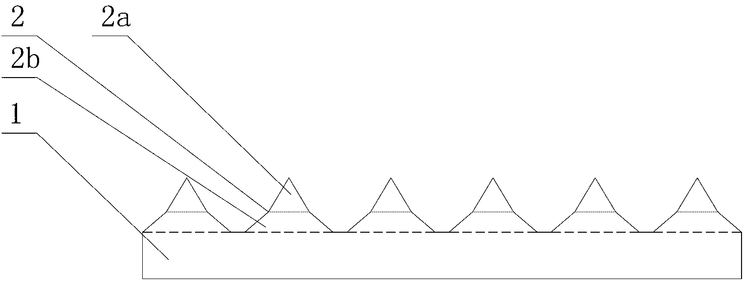
[0049] (3) Dry etching and wet etching are used to etch once respectively, the total etching depth is 1 μm, and pattern protrusions 2 are obtained by etching on the front side of the basic substrate 1, such as figure 1 As shown, the pattern protrusions 2 are arranged in an array on the front of the basic substrate 1, and the pattern protrusions 2 are composed of upper layer protrusions 2a and lower layer protrusions 2b, the bottom width of the upper layer protrusions 2a is the same as the top width of the lower layer pro...


PUM


Abstract

The invention relates to a patterned substrate which comprises a basic substrate. The front of the basic substrate is etched to form a patterned projection arranged in an array mode. The patterned substrate is characterized in that the patterned projection comprises a plurality of projections, the widths of the projections are progressively decreased from bottom to top, the width of the bottom of an upper projection is as same as that of the top of a lower projection, and the uppermost projection of the patterned projection is multilaterally conical, multilaterally cylindrical, multilaterally trapezoidal or multilaterally square table-shaped. The basic substrate is a sapphire substrate, a silicon carbide substrate or a silicon substrate. The patterned projection and the basic substrate are made of the same materials. The uppermost projection of the patterned projection and the basic substrate are made of different materials, the projections below the uppermost projection of the patterned projection and the basic substrate are made of the same materials, and the uppermost projection of the patterned projection is made of SiO2, Si3N4, ZnO2, Si or GaAs. A reflecting surface is added, multiple reflection of light inside the patterned substrate is decreased, and the light extraction efficiency of a chip can be effectively improved.

Description

technical field [0001] The invention relates to a graphic substrate and a preparation method thereof, belonging to the technical field of LED chip structures. Background technique [0002] Patterned Sapphire Substrate (PSS, Patterned Sapphire Substrate), which is to grow a mask for dry etching on a sapphire substrate, use a standard photolithography process to carve a pattern on the mask, and use ICP (Inductively Coupled Plasma, that is, induction Coupled plasma etching) technology to etch sapphire, remove the mask, and then grow GaN material on it, so that the vertical epitaxy of GaN material becomes lateral epitaxy. On the one hand, it can effectively reduce the dislocation density of the GaN epitaxial material, thereby reducing the non-radiative recombination of the active area, reducing the reverse leakage current, and improving the life of the LED; on the other hand, the light emitted by the active area passes through GaN and sapphire Multiple scattering at the interfa...

Claims


Application Information

Patent Timeline
Patent Type & Authority Applications(China)
IPC IPC(8): H01L33/10H01L33/22H01L33/00
Inventor 许南发黄慧诗
Owner SHANDONG NOVOSHINE OPTOELECTRONICS CO LTD
Why Eureka
Try Eureka