Photoinduced bending flexible electro-conductive baseplate and preparation method thereof

A photobending and flexible conductive technology, applied in the field of bionics, can solve the problems of no conductive substrate, failure of photobending actuators or robot integration and miniaturization, and achieve the effect of accelerating application

Inactive Publication Date: 2013-04-10
UNIV OF ELECTRONICS SCI & TECH OF CHINA
View PDF5 Cites 17 Cited by
  • Summary
  • Abstract
  • Description
  • Claims
  • Application Information

AI Technical Summary

Problems solved by technology

However, the current research is mainly based on the deformation of the film produced by photobending, which is then used as the power of the actuator. Usually, the lighting device is also an additional platform, so that the integration and miniaturization of photobending actuators or robots cannot be truly realized.
[0005] So far, there have not been any related reports on conductive substrates based on photobendable polymer materials.

Method used


Image

  • Photoinduced bending flexible electro-conductive baseplate and preparation method thereof

Examples


Embodiment 1

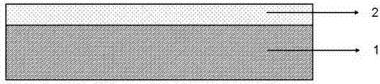
[0036] like figure 1 As shown, the photobending flexible substrate 1 of the substrate is a cross-linked liquid crystal polymer, the conductive layer 2 is carbon nanotubes, and the thickness of the conductive layer is 200 nm. The entire device structure is described as:

[0037] Cross-linked liquid crystal polymer / carbon nanotubes

[0038] The preparation method is as follows:

[0039] ① Use acetone, ethanol solution and deionized water to ultrasonically clean the surface of the glass substrate with a surface roughness less than 1 nm, and blow dry with dry nitrogen after cleaning.

[0040] ② The conductive layer of carbon nanotubes was prepared by spin-coating. The spin-coating speed was 1000 rpm, the duration was 30 s, and the film thickness was 200 nm. Then, the substrate was thermally annealed at 130 °C;

[0041] ③ Drop-coat the cross-linked liquid crystal polymer on the substrate, first heat the substrate to 100°C for 10 minutes. Then cool down to the clearing point of ...

Embodiment 2

[0046] like figure 1 As shown, the photobending flexible substrate 1 of the substrate is liquid crystal gel, the conductive layer is silver nanowires, and the thickness of the conductive layer is 180 nm. The entire device structure is described as:

[0047] Liquid crystal gel / silver nanowire

[0048] The preparation process is similar to Example 1.

Embodiment 3

[0050] like figure 1 As shown, the photobending flexible substrate 1 of the substrate is a liquid crystal elastomer, the conductive layer 2 is silver nanowires, and the thickness of the conductive layer is 160 nm. The entire device structure is described as:

[0051] Liquid crystal elastomer / gold nanowire

[0052] The preparation process is similar to Example 1.


PUM

PropertyMeasurementUnit
thicknessaaaaaaaaaa
surface roughnessaaaaaaaaaa
thicknessaaaaaaaaaa

Abstract

The invention discloses a photoinduced bending flexible electro-conductive baseplate and a preparation method thereof. The photoinduced bending flexible electro-conductive baseplate comprises a photoinduced bending flexible substrate and an electro-conductive layer, wherein the photoinduced bending flexible substrate is made of a photoinduced bending polymer material, and the electro-conductive layer is attached onto the surface of the photoinduced bending flexible substrate. The flexible baseplate simultaneously having the photoinduced bending capability and the electro-conductive capability is prepared, so that the integration and the microminiaturization of a photoinduced bending actuator and a light source can be realized, and the wide application and the quick development of a photoinduced bending material in the field of artificial muscles can be accelerated.

Description

technical field [0001] The invention belongs to the field of bionic technology, and in particular relates to a photoinduced bending flexible conductive substrate and a preparation method thereof. Background technique [0002] Since the middle of the 20th century, people have become more and more aware of the importance of the inspiration of nature for the development of new materials and technologies, thus proposing the concept of bionics and establishing the discipline of bionics. With the development of research, bionics has become a frontier and focus of natural science. Since the beginning of the 21st century, with the continuous deepening of robot development and people's strong demand for intelligent mechanical systems, artificial muscles, which are the key to driving robots and intelligent mechanical systems, have become the focus of bionics research. Muscle is a biologically contractile tissue with the functions of information transmission, energy transmission, wast...

Claims


Application Information

Patent Timeline
Patent Type & Authority Applications(China)
IPC IPC(8): B32B5/00B32B33/00B32B37/00H01B5/14H01B13/00
Inventor 陈珉于军胜马柱郑毅帆
Owner UNIV OF ELECTRONICS SCI & TECH OF CHINA
Why Eureka
Try Eureka