Solar cell wafer and printing screen thereof

A technology of solar cells and printing screens, which is applied in the field of solar cells, can solve problems such as roughness, silicon chip cracks, and hidden cracks, and achieve the effects of increasing the adjustment range, improving conversion efficiency, and uniform thickness

Active Publication Date: 2013-04-10
YINGLI ENERGY CHINA
View PDF6 Cites 8 Cited by
  • Summary
  • Abstract
  • Description
  • Claims
  • Application Information

AI Technical Summary

Problems solved by technology

However, during the sintering process of the back electrode, positive electrode and back electric field, there will be a phenomenon that the thinner edge area of ​​aluminum will form

Method used


Image

  • Solar cell wafer and printing screen thereof
  • Solar cell wafer and printing screen thereof
  • Solar cell wafer and printing screen thereof

Examples


Embodiment 1

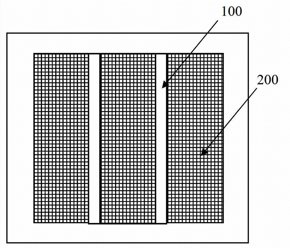
[0036] This embodiment provides a printing screen, its schematic diagram is as follows image 3 As shown, S000 represents the printing direction of the squeegee. Except for the non-hollowed part of the main grid S100, the screen meshes of the two edge hollowed out areas S200 parallel to the printing direction S000 are smaller than the screen meshes of other hollowed out areas S300, that is, each The screen mesh area of ​​the edge hollow area is smaller than the screen mesh area of ​​other hollow areas. Wherein, the wire mesh is a wire mesh or a non-metal mesh.

[0037] The two edge hollow areas of the silk screen described in this embodiment are the area 2mm-8mm away from the edge of the screen, including the endpoint value, and the mesh number of each edge hollow area is 250 mesh / cm-325 mesh / cm , the mesh number of other hollow areas is 350 mesh / cm-400 mesh / cm. That is to say, in the two edge hollow areas, the screen mesh area of ​​each edge hollow area is 0.31mm 2 -0.4mm ...

Embodiment 2

[0040] This embodiment provides a solar battery sheet, the aluminum back field of the solar battery sheet is printed using the printing screen described in the above embodiment, wherein the thickness of the aluminum back field of the entire solar battery sheet is uniform.

[0041]The preferred solar cells in this embodiment are N-type solar cells or P-type solar cells.

[0042] The aluminum back field of the solar cells in this embodiment is printed using the printing screen described in the above embodiments, so that the thickness of the aluminum back field printed on the entire silicon wafer is uniform, and the adjustment range of the sintering temperature is increased, so that the sintering temperature can be adjusted. By increasing the sintering temperature, the surface electrical contact ability between the front electrode, the back electrode and the back electric field of the solar cell is improved, and finally the conversion efficiency of the solar cell is improved.


PUM


Abstract

The invention discloses a solar cell wafer and a printing screen thereof. The number of the meshes of the two edge engraved areas of the printing screen parallel with the printing direction is less than the number of the meshes of the other engraved area. By changing the parameter of part of the edge engraved areas of the printing screen, the thickness of aluminium paste printed on the whole silicon wafer is enabled to be uniform, the surface of the edge area with thin aluminium is prevented from becoming rough or producing aluminium balls due to temperature fluctuation when sintering temperature is high, the sintering temperature regulation range is broadened, consequently, the surface electric contact capability between the front electrode, the back electrode and the back electric field of the solar cell wafer can be enhanced by increasing the sintering temperature, and thereby the conversion efficiency of a solar cell can be increased ultimately.

Description

technical field [0001] The invention relates to the technical field of solar cells, more specifically, to a solar cell sheet and its printing screen. Background technique [0002] In recent years, the production technology of solar cells has been continuously improved, the production cost has been continuously reduced, and the conversion efficiency has been continuously improved. The application of photovoltaic power generation has become increasingly popular and developed rapidly, and it has gradually become an important source of power supply. A solar cell is a photoelectric element with energy conversion, which can convert light energy into electrical energy under the irradiation of sunlight to realize photovoltaic power generation. [0003] As a clean and environmentally friendly new energy source, the application of solar cells is becoming more and more popular, but the production process of solar cells is relatively complicated. The current production process of solar ...

Claims


Application Information

Patent Timeline
IPC IPC(8): B41F15/36H01L31/0224
Inventor 范志东张小盼李倩赵学玲
Owner YINGLI ENERGY CHINA
Why Eureka
Try Eureka