Method for strip testing of mems devices, testing strip of mems devices and mems device thereof

A device and strip technology, applied in the field of MEMS device, its strip test and its test strip field

Active Publication Date: 2013-04-10
STMICROELECTRONICS SRL +1
View PDF11 Cites 6 Cited by
  • Summary
  • Abstract
  • Description
  • Claims
  • Application Information

AI Technical Summary

Problems solved by technology

[0013] Various solutions have been proposed to solve the problems related to the stresses acting on the devices in the form of strips and their electrical isolation

Method used


Image

  • Method for strip testing of mems devices, testing strip of mems devices and mems device thereof
  • Method for strip testing of mems devices, testing strip of mems devices and mems device thereof
  • Method for strip testing of mems devices, testing strip of mems devices and mems device thereof

Examples


Embodiment Construction

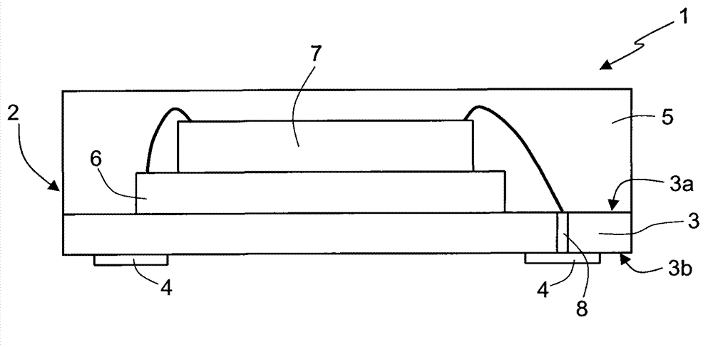
[0035] The present inventors have recognized that the co-mold compound surrounding the various MEMS devices in the test strip is responsible for residual stress acting on the same devices and skewing the testing process.

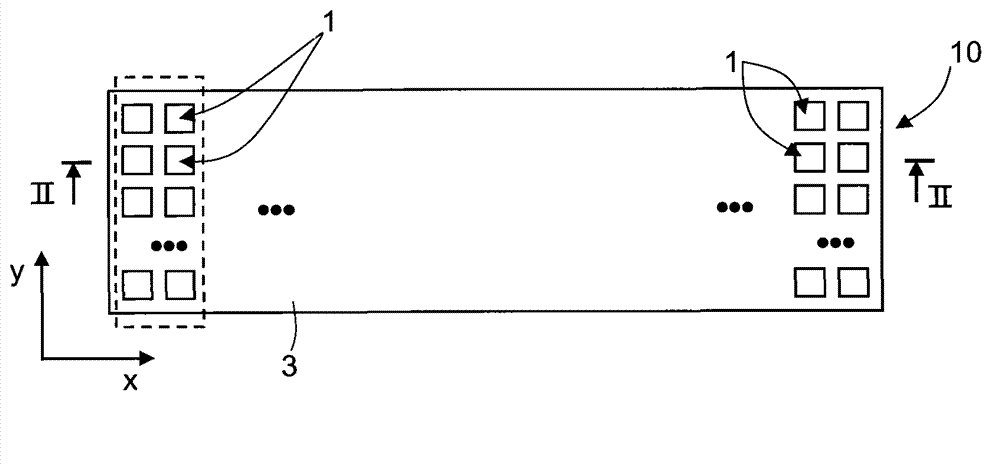
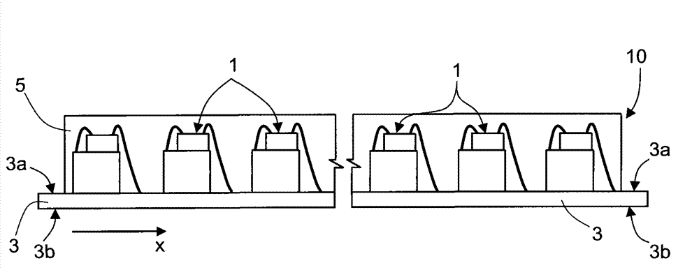
[0036] Therefore, if Figure 4 (where the same numerals denote the same elements as disclosed above, which will not be described hereinafter), a first aspect of the invention contemplates removing the surrounding strip, for example via a cutting or excision operation, prior to performing the test operation. 10 of the molding compound 5 for the entire thickness of the MEMS device 1 . The cutting performed also extends through the inner surface part of the substrate 3 (starting from the inner surface 3a on which the die of the MEMS device 1 is arranged), which part is removed so as to leave only a gap between the adjoining MEMS devices 1 between the remaining substrate portions indicated by 12. These remaining substrate portions 12 (consisting of the outer s...


PUM


Abstract

A method for testing a strip of MEMS devices, the MEMS devices including at least a respective die of semiconductor material coupled to an internal surface of a common substrate and covered by a protection material; the method envisages: detecting electrical values generated by the MEMS devices in response to at least a testing stimulus; and, before the step of detecting, at least partially separating contiguous MEMS devices in the strip. The step of separating includes defining a separation trench between the contiguous MEMS devices, the separation trench extending through the whole thickness of the protection material and through a surface portion of the substrate, starting from the internal surface of the substrate.

Description

technical field [0001] The present invention relates to a method for strip testing of MEMS (Micro Electro Mechanical Systems) devices, a test strip for MEMS devices and a MEMS device designed for the method. Background technique [0002] MEMS devices are playing an increasingly important role in the electronics industry, especially in the consumer electronics segment of portable electronic devices, due to their reduced size and power consumption. [0003] As is well known, a MEMS device comprises one or more dies of semiconductor material encapsulated in a package (for example, in the case of a MEMS sensor device, a first die integrates a mechanical sensing structure, while a second die integrates a physical Becoming the relevant electronic interface of the ASIC (Application Specific Integrated Circuit), the package protects and covers the die and provides suitable electrical connections to the outside (eg for soldering to an external printed circuit board). [0004] Common...

Claims


Application Information

Patent Timeline
Patent Type & Authority Applications(China)
IPC IPC(8): G01R31/00G01D5/12
CPCB81C99/004H01L24/97H01L2224/48091H01L2224/49109H01L2224/73265H01L2924/181H01L2924/00014H01L2924/00
Inventor M·阿佐帕迪C·卡奇雅S·波兹
Owner STMICROELECTRONICS SRL
Why Eureka
Try Eureka