Light emitting diode chip and preparation method thereof

A technology of light-emitting diodes and chips, applied in electrical components, circuits, semiconductor devices, etc., can solve the problems of current waste, waste, limited current expansion ability, etc. Effect

Active Publication Date: 2015-04-01
HC SEMITEK CORP
View PDF3 Cites 0 Cited by
  • Summary
  • Abstract
  • Description
  • Claims
  • Application Information

AI Technical Summary

Problems solved by technology

[0005] In the prior art, the current-expanding roots of the chip are manufactured by a lithography machine. Due to the control of manufacturing costs, the line width accuracy of the lithography machine used in production is generally above several microns, and the width of the current-expanding roots produced by it is also Above a few microns, since the current extension roots are opaque, the light extraction efficiency will be reduced. In order not to affect the light extraction efficiency, the number of current extension roots is usually set to be small, so that the current The ability to expand is limited; and, because the current expansion root is opaque, the light below it cannot be emitted to the outside of the chip, resulting in a waste of current. In order to avoid current waste, it is necessary to add a current blocking layer under the current expansion root. , so that the current on the current extension root does not spread to the area directly below it, which increases the complexity of the process and the manufacturing cost

Method used


Image

  • Light emitting diode chip and preparation method thereof
  • Light emitting diode chip and preparation method thereof
  • Light emitting diode chip and preparation method thereof

Examples


Embodiment 1

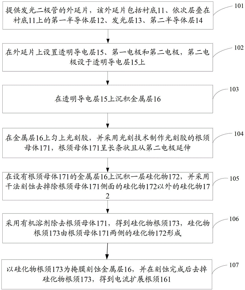
[0032] An embodiment of the present invention provides a method for manufacturing a light emitting diode chip, see figure 1 and figure 2 , the method includes:

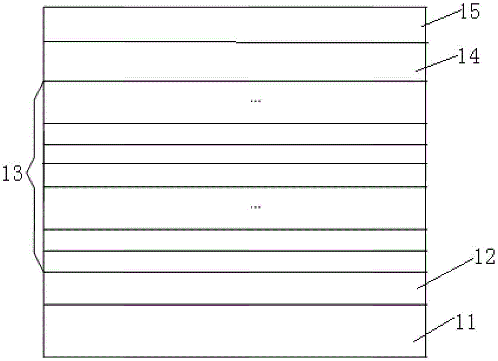
[0033] Step 101: providing an epitaxial wafer of a light emitting diode, the epitaxial wafer includes a substrate 11, a first semiconductor layer 12, a light emitting layer 13, and a second semiconductor layer 14 sequentially stacked on the substrate 11;

[0034] Specifically, the first semiconductor layer 12 may be an n-type doped GaN layer, the light emitting layer 13 may be an InGaN / GaN layer, and the second semiconductor layer 14 may be a p-type GaN layer.

[0035] Preferably, the first semiconductor layer 12 , the light emitting layer 13 and the second semiconductor layer 14 can be sequentially stacked and grown on the substrate 11 by metal organic chemical vapor deposition method.

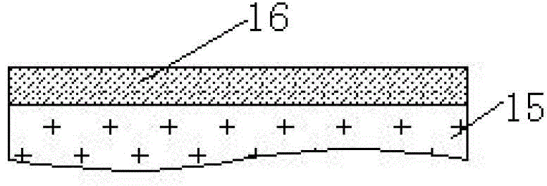
[0036] Step 102 : setting a transparent conductive layer 15 , a first electrode and a second electrode on the epitaxial wafer, a...

Embodiment 2

[0054] An embodiment of the present invention provides a light-emitting diode chip, which can be produced by the method for manufacturing a light-emitting diode chip provided in Example 1, see Figure 10 , the chip includes:

[0055] The epitaxial wafer and the first electrode 221 and the second electrode 241 arranged on the epitaxial wafer, the epitaxial wafer includes a substrate 21 and a first semiconductor layer 22 stacked on the substrate 21 in sequence, a light emitting layer (not shown), a second semiconductor layer layer 24 and a transparent conductive layer 25, the second electrode 241 is arranged on the transparent conductive layer 25, the second semiconductor layer 24 is directly arranged on the light-emitting layer, and a plurality of current spreading roots 242 are connected to the second electrode 241, and the current spreading roots The whiskers 242 have a width of 1 nm to 10 μm.

[0056] Preferably, the electrical conductivity of the current spreading roots 24...


PUM


Abstract

The utility model discloses a light emitting diode chip and a preparation method thereof, and belongs to the technical field of semiconductors. The preparation method includes that an epitaxial wafer of the light emitting diode chip is provided, a transparent conducting layer, a first electrode and a second electrode are arranged on the epitaxial wafer, the second electrode is arranged on the transparent conducting layer, a metal layer is arranged on the transparent conducting layer in a depositing mode, photoresist is evenly coated on the metal layer, a root hair matrix of the photoresist can be manufactured by using of photoetching technique, and the root hair matrix is in a long strip shape and extend from the second electrode. A layer of silicide is coated on the metal layer which is provided with the root hair matrix in a depositing mode. Silicide except silicide on the side face of the root hair matrix is removed by using dry etching. The dry etching is removed by using organic solvent so that silicide root hairs are obtained. The silicide root hairs are formed by the silicide on two sides of the root hair matrix and used as covering films to etch the metal layer and removed after etching is finished, so that current expanding root hairs are obtained. Through the scheme, current expanding capacity is improved.

Description

technical field [0001] The invention relates to the technical field of semiconductors, in particular to a light emitting diode chip and a manufacturing method thereof. Background technique [0002] Light-emitting diode chips are semiconductor wafers, which are the core components of light-emitting diodes. A light-emitting diode chip generally includes a substrate and a first semiconductor layer, a light-emitting layer, a second semiconductor layer, and a transparent conductive layer grown on the substrate in sequence. Metal electrodes (also known as punching electrodes) are respectively arranged on the first semiconductor layer and the transparent conductive layer. wire solder joints). Among them, the light emitting surface of the chip is a transparent conductive layer, and the transparent conductive layer can expand the current. In order to improve the uniformity of current expansion, the metal electrode on the transparent conductive layer of many chips is not only in the...

Claims


Application Information

Patent Timeline
Patent Type & Authority Patents(China)
IPC IPC(8): H01L33/14H01L33/38H01L33/00
Inventor 金迎春
Owner HC SEMITEK CORP
Why Eureka
Try Eureka