Complete forbidden band photonic crystal structure, preparation method of the same and luminous diode

A technology of light-emitting diodes and photonic crystals, applied in semiconductor devices, electrical components, circuits, etc., to reduce dislocation density, improve light extraction efficiency, and expand application value

Inactive Publication Date: 2013-04-10
SOUTHEAST UNIV
View PDF5 Cites 9 Cited by
  • Summary
  • Abstract
  • Description
  • Claims
  • Application Information

AI Technical Summary

Problems solved by technology

[0004] Technical problem: Aiming at the problems and deficiencies of the above-mentioned existing LEDs containing a single photonic crystal structure, the present invention provides a method to improve the light ex...

Method used


Image

  • Complete forbidden band photonic crystal structure, preparation method of the same and luminous diode
  • Complete forbidden band photonic crystal structure, preparation method of the same and luminous diode
  • Complete forbidden band photonic crystal structure, preparation method of the same and luminous diode

Examples


Embodiment Construction

[0034] The present invention will be further described below in conjunction with the accompanying drawings.

[0035]The main purpose of the invention is to solve the problems of low light extraction efficiency of existing LED devices and how to obtain high-quality GaN-based LED epitaxial films. According to the novel LED with complete photonic bandgap photonic crystal structure and its preparation method which can significantly increase the light extraction efficiency provided by the present invention, the above problems can be well solved. In addition, the structural parameters of the air hole type and dielectric column type photonic crystals that constitute the novel photonic crystal structure provided by the present invention can be adjusted independently and freely, and can be applied to various types of substrate materials and optoelectronic devices in light-emitting wavelength bands.

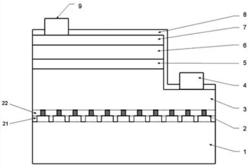
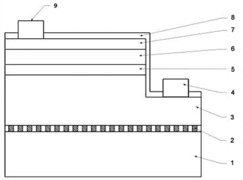
[0036] like Figure 5 Shown is the structural representation of the complete photonic ...


PUM

PropertyMeasurementUnit
Diameteraaaaaaaaaa
Heightaaaaaaaaaa

Abstract

The invention discloses a complete forbidden band photonic crystal structure. The complete forbidden band photonic crystal structure comprises an air-hole type photonic crystal structure located on the bottom layer and a dielectric-cylinder type photonic crystal structure located on the upper layer. The air-hole type photonic crystal structure and the dielectric-cylinder type photonic crystal structure are both arrays periodically arranged by dielectric materials with two or more than two dielectric constants on a plane. The dielectric material of dielectric-cylinder type photonic crystal structure is correspondingly arranged on the surface of the material of the air-hole type photonic crystal structure. A preparation method of the photonic crystal structure and a luminous diode adopting the photonic crystal structure are also disclosed. The photonic crystal structure has the advantages that a property of a complete photo forbidden band in an LED (light-emitting diode) light band is achieved, luminous efficiency of the LED is improved greatly, structural parameters of the photonic crystal can be adjusted freely, application value in the field of the LED is expanded, stress produced by lattice mismatch is released effectively, and GaN-based epitaxial thin films with higher quality is achieved.

Description

technical field [0001] The invention belongs to the field of semiconductor lighting, relates to a complete band-gap photonic crystal structure and a preparation method thereof, and also relates to a light-emitting diode adopting the complete band-gap photon crystal structure. Background technique [0002] At present, LEDs still have problems such as high cost, low luminous efficiency, and poor reliability, and the luminous efficiency of white LEDs is not high. These problems limit the application of LEDs in various fields. [0003] The electro-optical conversion efficiency of LED is determined by the internal quantum efficiency and light extraction efficiency. The current LED technology can improve the internal quantum efficiency of LED to a very high level, but the light extraction efficiency is not the same, and there is still a lot of room for improvement. So at this stage, one of the efforts of LED researchers is to improve the light extraction efficiency of LEDs. Both ...

Claims


Application Information

Patent Timeline
IPC IPC(8): H01L33/16H01L33/00
Inventor 张雄郭浩许洁崔一平
Owner SOUTHEAST UNIV
Why Eureka
Try Eureka