Novel metamaterial

A metamaterial, a new type of technology, applied in the field of materials, can solve problems such as high dielectric constant and inability to change the dielectric constant

Active Publication Date: 2013-04-10
KUANG CHI INST OF ADVANCED TECH +1
View PDF2 Cites 3 Cited by
  • Summary
  • Abstract
  • Description
  • Claims
  • Application Information

AI Technical Summary

Problems solved by technology

[0005] The technical problem to be solved by the present invention is to provide a new type of metamaterial for the above-mentioned defects that the dielectric constant of the material in the prior art is relatively high, cannot reach or a

Method used


Image

  • Novel metamaterial
  • Novel metamaterial
  • Novel metamaterial

Examples


Embodiment 1

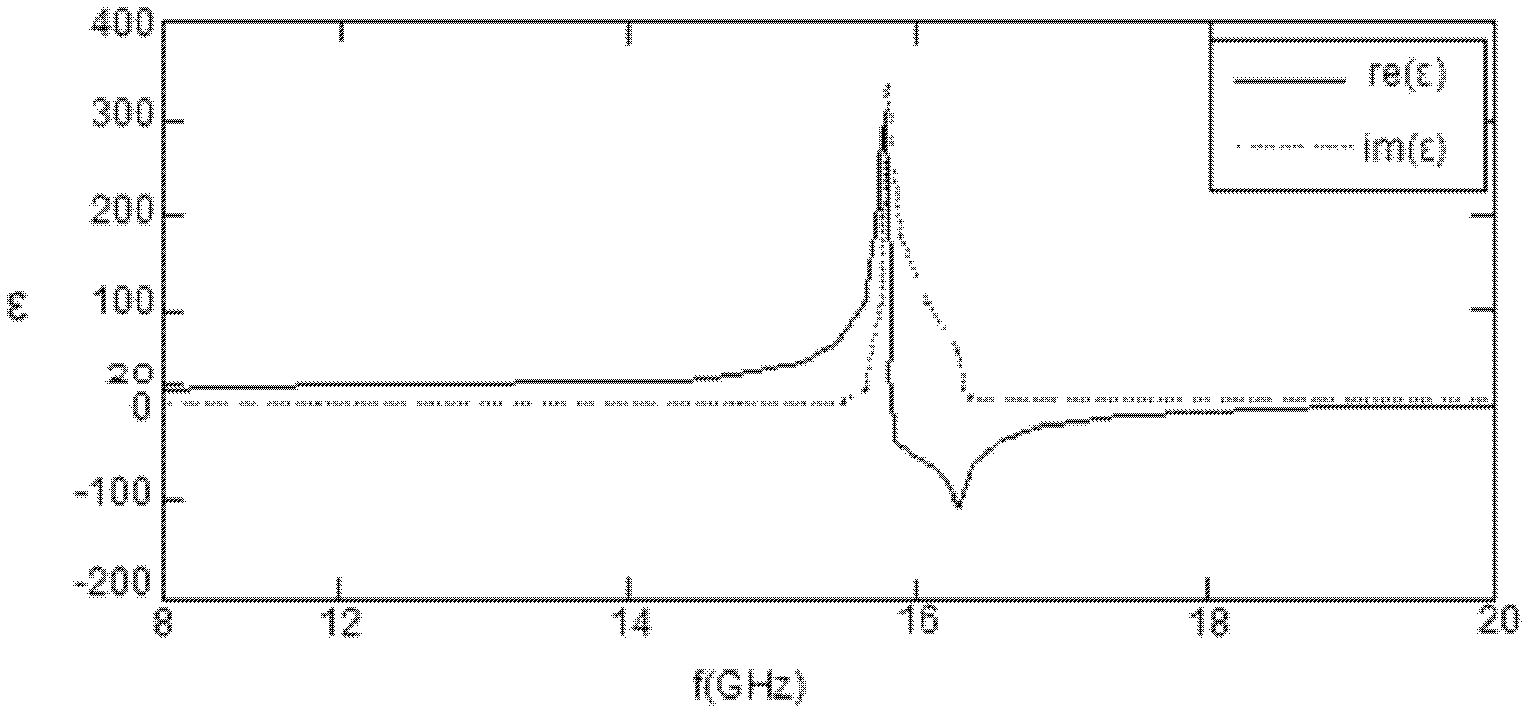
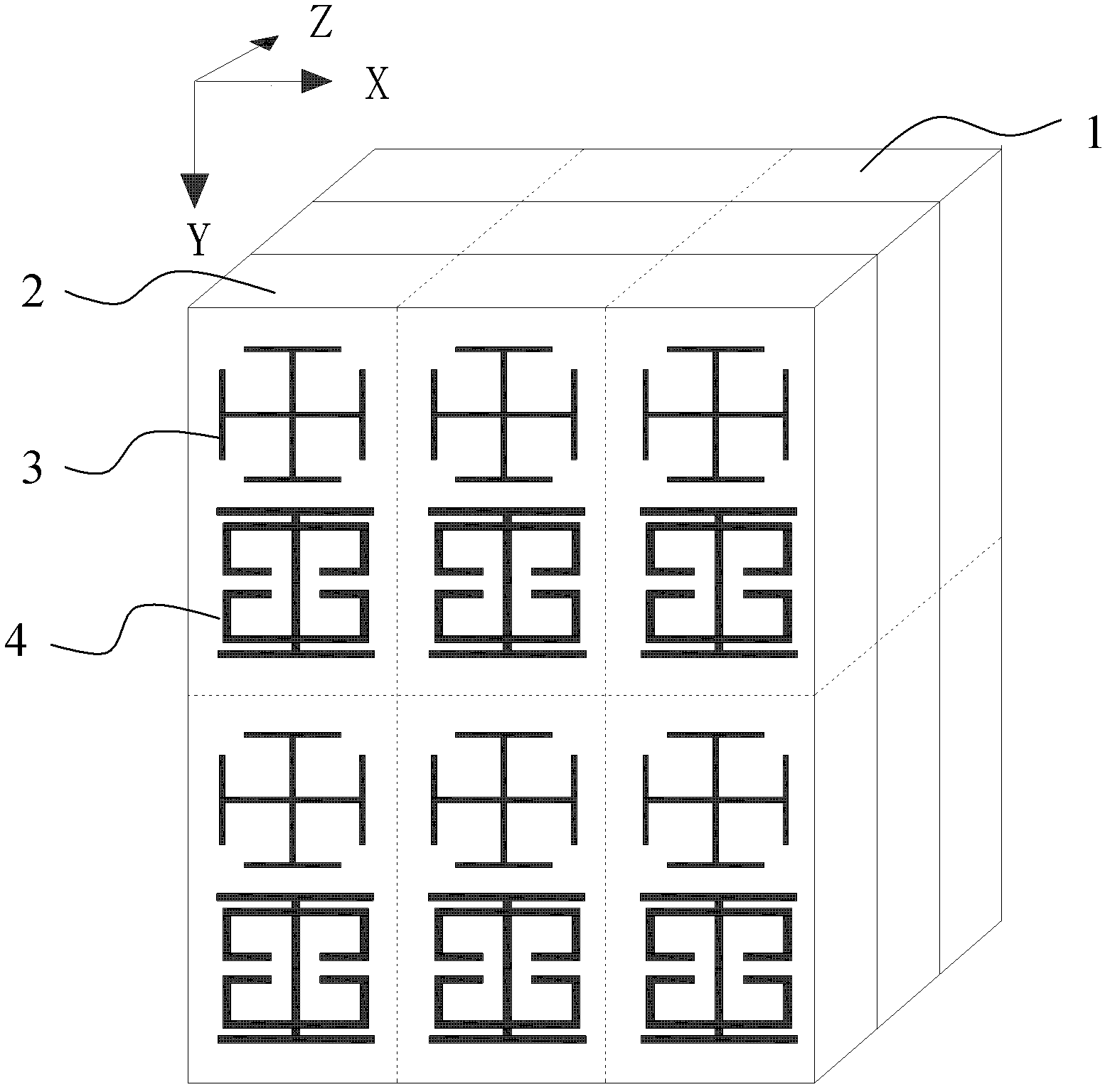
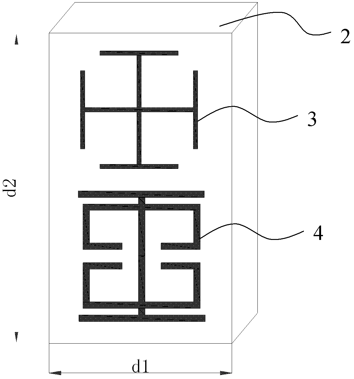
[0033] When the first artificial microstructure 3 such as Figure 4 As shown, a1=0.4 mm, a2=0.1 mm, a3=0.8 mm, the second artificial microstructure 4 is as Figure 5 As shown, b1=1.8 mm, b2=0.1 mm, b3=0.7 mm, b4=0.6 mm, the substrate unit is as image 3 As shown, d1 = 2 mm, d2 = 4 mm, and the thickness is 0.4 mm. The simulation diagram obtained by using the above parameters is as follows Figure 7 shown by Figure 7 The solid line in the figure shows that the metamaterial has multiple resonance peaks, and the dielectric constant gradually increases from zero in a certain frequency band (20.3GHz-22.8GHz, 30GHz-34.3GHz), and the dielectric constant of 0-17GHz in another frequency band The constant change is relatively stable and has a large value, and it can be seen from the dotted line that the imaginary part of the corresponding dielectric constant is close to zero in the above-mentioned frequency band with a small dielectric constant, so the loss is also low.

Embodiment 2

[0035] The difference from Embodiment 1 lies in the size of the first artificial microstructure 3. The first artificial microstructure 3 after the size increase is as follows: Figure 6 As shown, c1=1.2 mm, c2=0.1 mm, c3=0.8 mm, the second artificial microstructure 4 is as Figure 5 As shown, b1=1.8 mm, b2=0.1 mm, b3=0.7 mm, b4=0.6 mm, such as image 3 For the substrate unit shown, d1=2 mm, d2=4 mm, and the thickness is 0.4 mm, the simulation diagram obtained by using the above parameters is as follows Figure 8 shown by Figure 8The solid line in the figure shows that the material still has multiple resonance peaks, and the dielectric constant gradually increases from zero in a certain frequency band (16.7GHz-19.3GHz, 27.1GHz-34.1GHz), and it can be seen from the dotted line that when the dielectric constant is relatively The imaginary part of the corresponding dielectric constant in the small above-mentioned frequency band is close to zero, so the loss is also low.

[003...


PUM


Abstract

The invention relates to a novel metamaterial which comprises at least one material plate layer. Each material plate layer comprises a substrate and artificial microstructures attached onto the substrate. The substrate is virtually divided into a plurality of substrate units arranged in array mode. A pair of artificial microstructures is attached onto each substrate unit. First artificial microstructures are of snowflake-shaped structures. Each second artificial microstructure comprises a first open ring structure, a second open ring structure and an I-shaped structure. Each I-shaped structure comprises a first metal line, a second metal line and a third metal line, wherein the first metal line and the second metal line are parallel to each other, and two ends of the third line are connected with the first metal line and the second metal line respectively. The third metal lines penetrate through the first open ring structures and the second open ring structures. The material has broadband high dielectric constant in a certain frequency band, has distribution of dielectric constants gradually increasing from zero in another frequency band and can meet requirements of a specific situation.

Description

technical field [0001] The present invention relates to a material, and more particularly, to a new type of metamaterial. Background technique [0002] Metamaterial, also known as artificial electromagnetic material, is a new type of artificial synthetic material, which is composed of a substrate made of non-metallic materials and multiple artificial microstructures attached to the surface of the substrate or embedded in the interior of the substrate. The substrate can be virtually divided into multiple substrate units arranged in a rectangular array. Each substrate unit is attached with artificial microstructures to form a metamaterial unit. The entire metamaterial is composed of many such metamaterial units, just like Crystals are composed of countless crystal lattices arranged in a certain way. The artificial microstructures on each metamaterial unit may or may not be identical. Artificial microstructures are planar or three-dimensional structures with certain geometric...

Claims


Application Information

Patent Timeline
IPC IPC(8): H01Q15/00
Inventor 刘若鹏栾琳寇超锋张岭
Owner KUANG CHI INST OF ADVANCED TECH
Why Eureka
Try Eureka