Array substrate, manufacture method of array substrate, liquid crystal display panel and display device

A technology of an array substrate and a manufacturing method, which is applied in the field of liquid crystal display to achieve the effects of increasing turn-on current, increasing Ion, and reducing channel length

Inactive Publication Date: 2013-04-17
BOE TECH GRP CO LTD
View PDF5 Cites 12 Cited by
  • Summary
  • Abstract
  • Description
  • Claims
  • Application Information

AI Technical Summary

Problems solved by technology

[0003] In the prior art, the source electrode and the drain electrode are located on the same layer and are formed at the same time through a single patterning process. Due to the constraints of t

Method used


Image

  • Array substrate, manufacture method of array substrate, liquid crystal display panel and display device
  • Array substrate, manufacture method of array substrate, liquid crystal display panel and display device
  • Array substrate, manufacture method of array substrate, liquid crystal display panel and display device

Examples


Embodiment 1

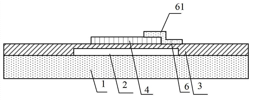
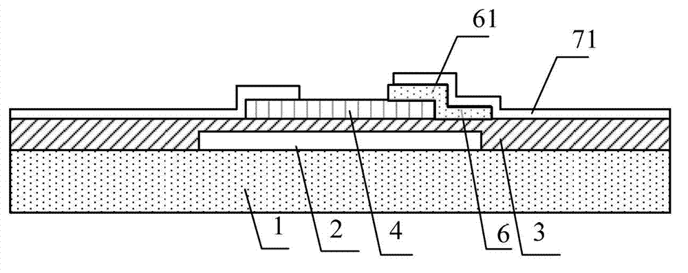
[0143] In this embodiment, the source electrode and the drain electrode are located in different layers, and are formed separately through two patterning processes, wherein the source electrode is formed first and then the drain electrode is formed, as Figure 2-11 As shown, the manufacturing method of the array substrate of this embodiment includes the following steps:

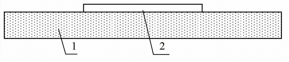
[0144] Step a1: provide a substrate 1, and form a pattern of gate electrodes and gate lines composed of a gate metal layer 2 on the substrate 1 through the first patterning process;

[0145] Specifically, the substrate 1 may be a transparent substrate. Such as figure 2 As shown, a gate metal layer 2 is first deposited on a substrate 1, and then patterns of gate electrodes and gate lines are formed through a first patterning process. Specifically, a gate metal layer 2 can be deposited on the substrate 1 by magnetron sputtering, wherein the gate metal layer 2 can be any one of Nd, Cr, W, Ti, Ta, Mo, Al and C...

Embodiment 2

[0165] In this embodiment, the drain electrode and the source electrode are located in different layers, and are respectively formed through two patterning processes, wherein the drain electrode is formed first and then the source electrode is formed. The manufacturing method of the array substrate of this embodiment includes the following steps:

[0166] Step b1: provide a substrate, and form a pattern of gate electrodes and gate lines consisting of a gate metal layer on the substrate through the first patterning process;

[0167] Specifically, the substrate may be a transparent substrate. A gate metal layer is first deposited on the substrate, and then patterns of gate electrodes and gate lines are formed through the first patterning process. Specifically, a gate metal layer can be deposited on the substrate by magnetron sputtering, wherein the gate metal layer can be any one of Nd, Cr, W, Ti, Tb, Mo, Bl and Cu or at least two of them Metal alloy; after that, a photoresist ...


PUM


Abstract

The invention provides an array substrate, a manufacture method of the array substrate, a liquid crystal display panel and a display device, and belongs to the field of liquid crystal display. A source electrode and a drain electrode of the array substrate are located at different layers. In the manufacture method of the array substrate, the source electrode and the drain electrode located at different layers are respectively formed through twice picture composition processes. By adopting the array substrate, the manufacture method of the array substrate, the liquid crystal display panel and the display device, the channel length between the source electrode and the drain electrode can be reduced as far as possible, and further starting current Ion of thin film transistors (TFTs) is greatly improved.

Description

technical field [0001] The invention relates to the field of liquid crystal display, in particular to an array substrate and a manufacturing method thereof, a liquid crystal display panel and a display device. Background technique [0002] Turn on current I on It is the most important parameter in TFT-LCD (thin film transistor-liquid crystal display), and its size directly affects the display quality of TFT-LCD. At present, since TFT-LCD is developing towards high refresh rate and high resolution, this requires TFT to have a relatively high turn-on current I on . For a-Si TFT, increase the turn-on current I on The main way is to increase the width-to-length ratio (W / L) of the channel. [0003] In the prior art, the source electrode and the drain electrode are located on the same layer, and are formed simultaneously through a single patterning process. Due to the constraints of the critical dimensional accuracy of the mask, the minimum channel length in the existing proce...

Claims


Application Information

Patent Timeline
IPC IPC(8): G02F1/1368G02F1/1362H01L21/77
CPCH01L29/41733H01L29/66765H01L29/78669
Inventor 张春芳金熙哲魏燕徐超
Owner BOE TECH GRP CO LTD
Why Eureka
Try Eureka