
Stage-matching-adjustable CMOS (complementary metal oxide semiconductor) ultra-wideband low-noise amplifier circuit

A low-noise amplifier, inter-stage matching technology, applied in the direction of improving the amplifier to expand the bandwidth, improving the amplifier to reduce the noise impact, etc. problems such as poor performance, to achieve the effect of simple structure, high gain flatness, and low cost

Active Publication Date: 2013-04-17
SHANGHAI INST OF MICROSYSTEM & INFORMATION TECH CHINESE ACAD OF SCI
View PDF5 Cites 23 Cited by
  • Summary
  • Abstract
  • Description
  • Claims
  • Application Information

AI Technical Summary

Problems solved by technology

For the common-gate input structure, the gain is not high, and the noise of the subsequent stage circuit cannot be well suppressed, especially in short-channel devices, the system noise is high, and the power consumption required is relatively large; while the parallel connection in the traditional sense The common source structure of resistance feedback, due to the influence of parasitic parameters, has poor performance in the high frequency band; and the use of current multiplexing technology can increase the gain in the high frequency band, but it is limited to the frequency requirements of ultra-wideband, and the gain flatness in the entire frequency band hard to get a guarantee

Method used


Image

  • Stage-matching-adjustable CMOS (complementary metal oxide semiconductor) ultra-wideband low-noise amplifier circuit
  • Stage-matching-adjustable CMOS (complementary metal oxide semiconductor) ultra-wideband low-noise amplifier circuit
  • Stage-matching-adjustable CMOS (complementary metal oxide semiconductor) ultra-wideband low-noise amplifier circuit

Examples


Embodiment Construction

[0024] The implementation of the present invention will be illustrated by specific specific examples below, and those skilled in the art can easily understand other advantages and effects of the present invention from the contents disclosed in this specification.

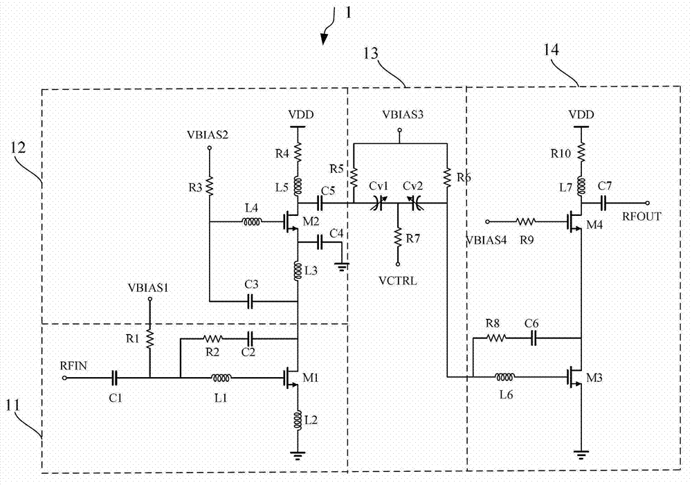
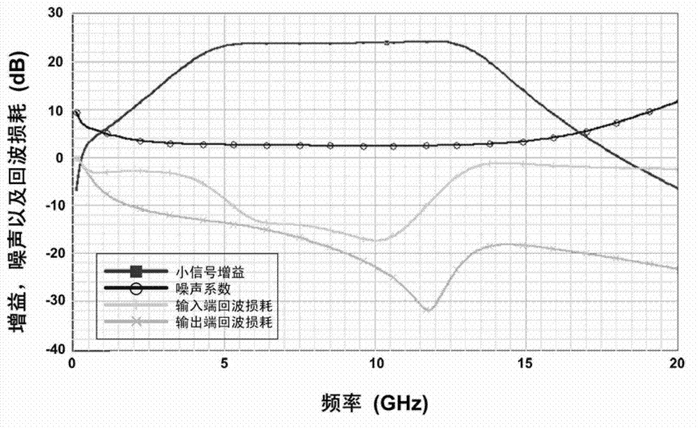
[0025] see Figure 1 to Figure 2 . It should be noted that the structures, proportions, sizes, etc. shown in the drawings attached to this specification are only used to match the content disclosed in the specification, for those who are familiar with this technology to understand and read, and are not used to limit the implementation of the present invention. Limiting conditions, so there is no technical substantive meaning, any modification of structure, change of proportional relationship or adjustment of size, without affecting the effect and purpose of the present invention, should still fall within the scope of the present invention. The disclosed technical content must be within the scope covered. At the sa...


PUM


Abstract

The invention provides a stage-matching-adjustable CMOS (complementary metal oxide semiconductor) ultra-wideband low-noise amplifier circuit which at least comprises a signal access circuit, a signal extraction circuit, a stage matching circuit and a second-stage amplifying circuit. The signal access circuit realizes matching of ultra-wideband input signals on the basis of a negative feedback circuit connected with a first MOS (metal oxide semiconductor) tube; the signal extraction circuit and the signal access circuit jointly form a first-stage amplifying circuit, signals outputted by the signal access circuit are extracted to a second MOS tube on the basis of a high-frequency matching circuit and a low-frequency matching circuit, the high-frequency matching circuit is connected with the first MOS tube and the second MOS tube, and the low-frequency matching circuit is connected with the second MOS tube; signals outputted by the signal extraction circuit are coupled by the stage matching circuit on the basis of adjustable capacitors; and signals outputted by the stage matching circuit are amplified by the second-stage amplifying circuit on the basis of common-source and common-gate circuits. The stage-matching-adjustable CMOS ultra-wideband low-noise amplifier circuit has the advantages of low noise, power consumption, fabrication error influence and cost, high gain and gain flatness, ultra-wide bandwidth, simple structure and the like, and is applicable to UWB (ultra wideband) communication systems.

Description

technical field [0001] The invention relates to the field of integrated circuits, in particular to a CMOS ultra-wideband low-noise amplifier circuit with adjustable inter-stage matching. Background technique [0002] Ultra-wideband (UWB) technology originated in the late 1950s, and was mainly used as a military technology in communication equipment such as radar. With the rapid development of wireless communication, people have put forward higher requirements for high-speed wireless communication, and ultra-wideband technology has been proposed again, and has attracted much attention. UWB technology is a technology that uses extremely short pulse signals to transmit information, and usually the duration of each pulse is only between tens of picoseconds and hundreds of picoseconds. The bandwidth that these pulses can provide is as high as several GHz, so the maximum data transmission rate can reach hundreds of Mbps; moreover, UWB is a high-speed and low-power data communicat...

Claims


Application Information

Patent Timeline
IPC IPC(8): H03F1/26H03F1/42
Inventor 李凌云叶禹孙晓玮
Owner SHANGHAI INST OF MICROSYSTEM & INFORMATION TECH CHINESE ACAD OF SCI
Learn More