Standard SiGe bipolar complementary metal-oxide-semiconductor transistor (BiCMOS) process-based optoelectronic integrated receiver

An optoelectronic integration and receiver technology, applied in electromagnetic receivers, radiation control devices, etc., can solve the problem that photoelectric detectors are difficult to take into account the performance of speed and responsivity at the same time, optoelectronic integrated receivers have not entered the practical stage, and monolithic integrated optics are limited. The overall performance of the receiver and other issues can achieve good application prospects, enhanced functions, and high responsiveness.

Inactive Publication Date: 2014-04-02
TIANJIN UNIV
View PDF3 Cites 11 Cited by
  • Summary
  • Abstract
  • Description
  • Claims
  • Application Information

AI Technical Summary

Problems solved by technology

However, limited by the indirect bandgap characteristics of the silicon material itself and the process structure, it is difficult for the photodetectors prepared by the standard CMOS process to take into account the performance of both speed and responsivity.
The bandwidth of conventional structure detectors is only tens of MHz, which severely limits the overall performance of monolithic integrated optical receivers
In addition, silicon-based detectors based on standard CMOS processes cannot detect the two important communication bands of 1310nm and 1550nm
Therefore, so far, optoelectronic integrated receivers based on standard CMOS technology have not yet entered the practical stage.

Method used


Image

  • Standard SiGe bipolar complementary metal-oxide-semiconductor transistor (BiCMOS) process-based optoelectronic integrated receiver
  • Standard SiGe bipolar complementary metal-oxide-semiconductor transistor (BiCMOS) process-based optoelectronic integrated receiver
  • Standard SiGe bipolar complementary metal-oxide-semiconductor transistor (BiCMOS) process-based optoelectronic integrated receiver

Examples


Embodiment Construction

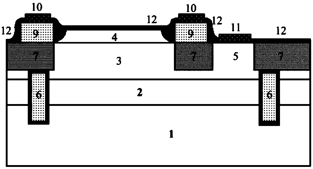
[0024] 1. The photodetector proposed by the present invention can make full use of the structural characteristics of the SiGe BiCMOS process to construct various detector structures such as PN junction, PIN, MSM and phototransistor, and can also use the silicon germanium epitaxial layer to improve the responsivity of the detector .

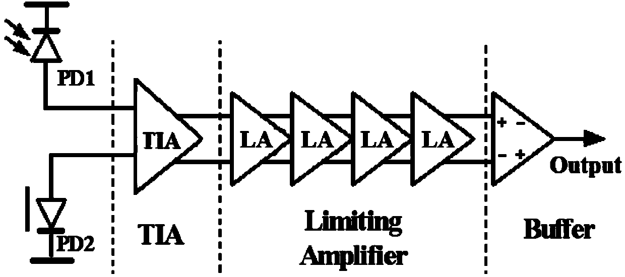
[0025] 2. The optical receiver front-end circuit based on the standard SiGe BiCMOS process proposed by the present invention comprises:

[0026] Two photodetectors with completely symmetrical structures, one of which converts the optical signal input by the optical fiber into a current signal, and the other detector is used to maintain the input load balance of the differential circuit and increase the bandwidth of the receiver;

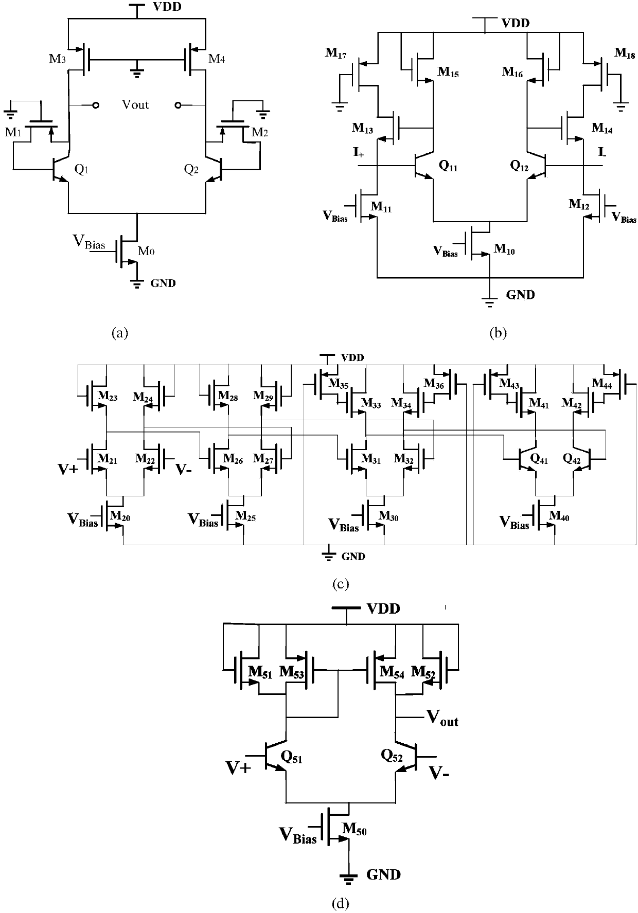
[0027] A transimpedance amplifier with a fully differential structure, its function is to convert the current signal output by the photodetector into a voltage signal, and perform preliminary amplification;

[0028] A s...


PUM


Abstract

The invention belongs to the fields of optical fiber communication systems and optical interconnection, and aims to achieve the advantages of small size, low cost, high reliability, rich functions and the like of monolithic integration. The invention provides a photoelectric detector compatible with a standard SiGe bipolar complementary metal-oxide-semiconductor transistor (BiCMOS) process, and a high-speed and high-sensitivity monolithic integrated optical receiver integrated with the detector. To meet the technical requirements, the standard SiGe BiCMOS process-based optoelectronic integrated receiver comprises two photoelectric detectors with completely symmetrical structures, a trans-impedence amplifier with a full differential structure, a group of sequentially cascaded full differential limiting amplifier and an output buffer stage which is used for converting differential voltage signals output by the limiting amplifier into single-end output voltage signals and providing driving force. The optoelectronic integrated receiver is mainly applied to design and manufacture of the optical fiber communication systems.

Description

technical field [0001] The invention belongs to the field of optical fiber communication systems and optical interconnection, and relates to a photoelectric detector compatible with silicon germanium bipolar-complementary metal oxide semiconductor (SiGe BiCMOS) technology, and a high-speed optical receiver monolithically integrating the detector. Specifically, it relates to a photoelectric integrated receiver based on a standard SiGe BiCMOS process. Background technique [0002] With the continuous development of communication and multimedia technology, people's demand for data information continues to increase. Because optical fiber communication has the advantages of high speed and large capacity, it is widely used in trunk network. However, for user terminals, limited by the cost of optoelectronic integrated chips, it is difficult to continue to advance the "last mile" of fiber-to-the-home. Therefore, the development of low-cost, high-performance optoelectronic integrat...

Claims


Application Information

Patent Timeline
Patent Type & Authority Applications(China)
IPC IPC(8): H04B10/60H01L27/144
Inventor 谢生毛陆虹郭增笑付友康玉琢
Owner TIANJIN UNIV
Why Eureka
Try Eureka