Image sensor wafer bonding method

A sensor and device wafer technology, applied in the field of image sensor wafer bonding, can solve problems such as difficult planarization, uneven surface, difficult chemical mechanical polishing, etc., to achieve the effect of achieving flatness and solving voids

Active Publication Date: 2013-04-24
WUHAN XINXIN SEMICON MFG CO LTD
View PDF3 Cites 8 Cited by
  • Summary
  • Abstract
  • Description
  • Claims
  • Application Information

AI Technical Summary

Problems solved by technology

In this process, after high-density plasma chemical vapor deposition oxidation (thickness is generally 16000-24000 angstroms), the surface will be more uneven, which will cause difficulties for chemical mechanical polishing, and it is not easy to achieve global flatness change

Method used


Image

  • Image sensor wafer bonding method
  • Image sensor wafer bonding method

Examples


Embodiment Construction

[0015] The principles and features of the present invention are described below in conjunction with the accompanying drawings, and the examples given are only used to explain the present invention, and are not intended to limit the scope of the present invention.

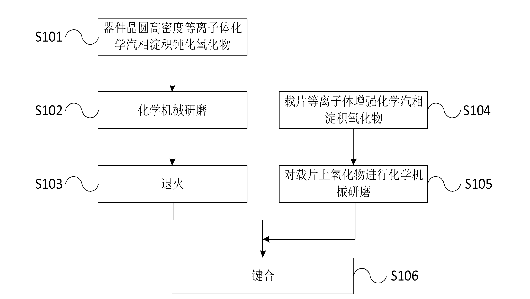
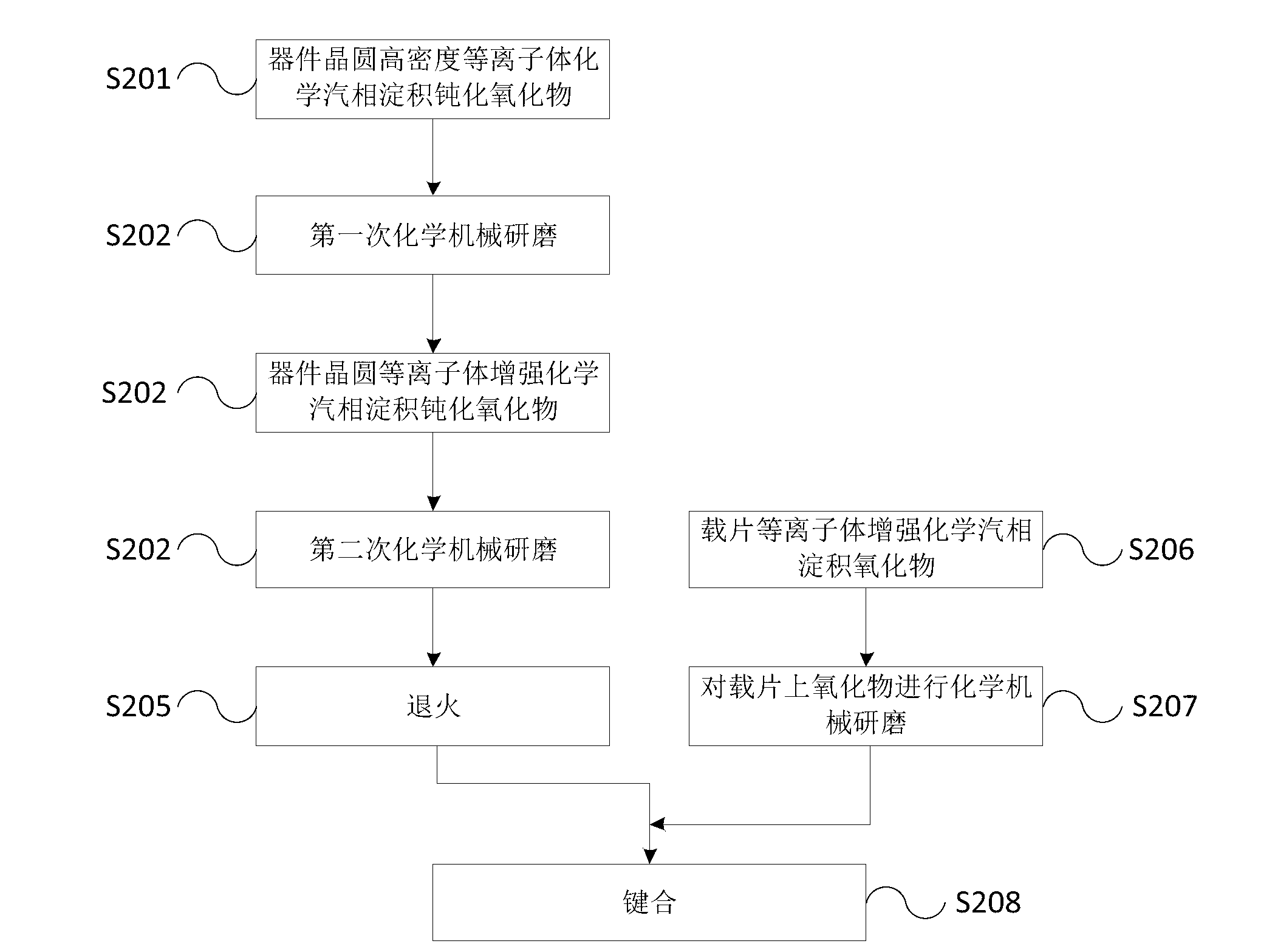
[0016] Such as figure 1 It is a flow chart of the existing image sensor wafer bonding process. It can be seen from the figure that the image sensor wafer bonding steps in the prior art, first, after step s101, the device wafer is deposited by high-density plasma chemical vapor deposition After passivating the oxide, step s102 grinds the oxide layer of the device wafer that has passed step s101, and then returns the device wafer through step s103, and step s104 is plasma-enhanced chemical vapor deposition of oxide on the carrier, Carrying out step s105 on the carrier that has passed step s104 to perform chemical mechanical polishing on the oxide on the carrier, and finally, bonding the treated and device wafer to the...


PUM


Abstract

The invention relates to the field of semiconductor manufacturing, in particular to an image sensor wafer bonding method. The image sensor wafer bonding method includes a first step of utilizing the high-density plasma chemistry vapor deposition technique to deposit passivation layer oxide on a device wafer, a second step of carrying out a first chemical mechanical lapping to the device wafer with the deposited passivation layer oxide, a third step of depositing the passivation layer oxide again on the original oxide of the device wafer through adoption of the plasma chemistry vapor deposition technique, a fourth step of carrying out a second chemical mechanical lapping to the device wafer, a fifth step of carrying out annealing treatment to the device wafer after the second chemical mechanical lapping, and a sixth step of bonding the treated device wafer and a ground slide which is subjected to the plasma enhanced chemistry vapor deposition oxide treatment and the chemical mechanical lapping. The image sensor wafer bonding method has the advantages that the plasma enhanced chemistry vapor deposition and the second chemical mechanical lapping are added to the device wafer after the original first chemical mechanical lapping, and consequently the plainness of the surface of the wafer is more effectively achieved, and the problem that holes are likely to generate after bonding is solved.

Description

technical field [0001] The invention relates to the field of semiconductor manufacturing, in particular to a bonding method of an image sensor wafer. Background technique [0002] Wafer bonding technology refers to the method of tightly combining two wafers through chemical and physical effects. Wafer bonding is often combined with surface silicon processing and used in the processing technology of micro-electromechanical systems. Although wafer bonding is not a direct means of micromachining, it plays an important role in micromachining. By combining with other processing methods, it can provide support and protection for microstructures, and can realize mechanical structure or mechanical structure and mechanical structure. An electrical connection between circuits. The quality of wafer bonding has a direct impact on the performance of the MEMS. [0003] The flatness of the bonded oxide for back-illuminated image sensors is critical for bonding. If the wafer surface is un...

Claims


Application Information

Patent Timeline
Patent Type & Authority Applications(China)
IPC IPC(8): H01L21/02
Inventor 李平
Owner WUHAN XINXIN SEMICON MFG CO LTD
Why Eureka
Try Eureka