Image sensor wafer reverse side processing method
An image sensor, backside processing technology, applied in radiation control devices and other directions, can solve the problems of crosstalk, high process temperature, high cost, etc., and achieve the effect of avoiding crosstalk, low temperature, and low cost
- Summary
- Abstract
- Description
- Claims
- Application Information
AI Technical Summary
Problems solved by technology
Method used
Image
Examples
Embodiment Construction
[0017] The principles and features of the present invention are described below in conjunction with the accompanying drawings, and the examples given are only used to explain the present invention, and are not intended to limit the scope of the present invention.
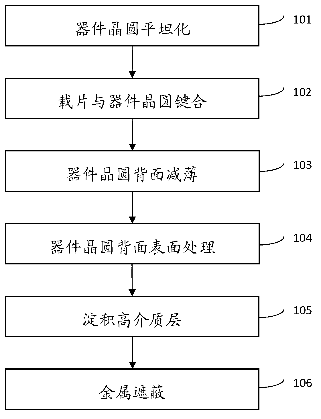
[0018] Such as figure 1 As shown, the backside processing of the image sensor wafer includes,
[0019] Step 101: polishing the surface of the wafer to make it planar;
[0020] Step 102: bonding and connecting the front side of the wafer to the carrier; Step 103: thinning the back side of the wafer;
[0021] Step 104: Treat the back surface of the wafer with ozone, wherein the ozone concentration is 20-80 mg / L (mg / L), and the treatment time is 6-15 minutes (minutes). After the treatment, an oxide film is formed on the back of the wafer , the oxide film thickness is 10-15 Angstroms (A);
[0022] Step 105: Deposit a high dielectric layer on the oxide film formed on the back of the wafer;
[0023] Step 106: Deposit ...
PUM
 Abstract
Description
Claims
Application Information
