Solar cell chip and manufacturing method thereof

A solar cell and chip technology, applied in circuits, photovoltaic power generation, electrical components, etc., can solve problems such as increasing the contact resistance between electrodes and semiconductor layers, limiting the contact area between electrodes and semiconductor layers, shortening the circulation distance, and improving sunlight utilization rate, improve the effect of conductivity

Active Publication Date: 2016-04-20
TIANJIN SANAN OPTOELECTRONICS
View PDF5 Cites 0 Cited by
  • Summary
  • Abstract
  • Description
  • Claims
  • Application Information

AI Technical Summary

Problems solved by technology

Traditional solar cells usually use a grid electrode structure, and the electrode grid lines form ohmic contact with the semiconductor layer. In order to maximize the use of sunlight, the total area of ​​the grid electrode accounts for only a small part of the total area of ​​the battery chip (less than 10%) ), which greatly limits the contact area between the electrode and the semiconductor layer, thereby increasing the contact resistance between the electrode and the semiconductor layer

Method used


Image

  • Solar cell chip and manufacturing method thereof
  • Solar cell chip and manufacturing method thereof
  • Solar cell chip and manufacturing method thereof

Examples


Embodiment Construction

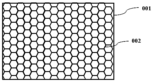
[0031] The following embodiments disclose a high-power concentrating solar cell chip and its manufacturing method. It uses transparent conductive materials to form ohmic contact with the battery semiconductor layer in a large area. Specifically, a grid-shaped metal nanometer is formed on the surface of the battery semiconductor layer Electrodes, and then cover the transparent conductive layer, so that the metal nano-electrodes are embedded in the transparent conductive layer, which greatly improves the conductivity of the conductive layer.

[0032] The following will be further described in conjunction with the implementation of the present invention, but the protection scope of the present invention should not be limited thereby.

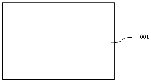
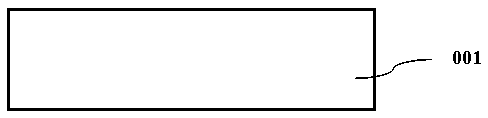
[0033] Such as figure 1 and figure 2 As shown, a high-power concentrated solar cell epitaxial wafer 001 is provided. Taking the GaInP / GaAs / Ge triple-junction solar cell as an example, the epitaxial layer of the GaInP / GaAs / Ge triple-junction cell...


PUM


Abstract

Provided is a high concentration solar cell chip, comprising: a solar cell epitaxial laminate layer (001); a grid-shaped metal nano-electrode (002) overlaid on the surface of the solar cell epitaxial laminate layer (001); a gate electrode (003) formed on the grid-shaped metal nano-electrode (002); and a transparent conductive layer (004) formed on the grid-shaped metal nano-electrode (002) and forming an ohmic contact with the solar cell epitaxial laminate layer(001). The solar cell chip employs a transparent conductive layer to form a large area ohmic contact with the surface of a cell epitaxial sheet, thus greatly reducing the contact resistance between an electrode and the cell epitaxial sheet; embedding a grid-shaped metal nano-electrode in the transparent conductive layer dramatically improves the conductivity of the transparent conductive layer, and solves the problem of deficient conductivity of the transparent conductive layer; improvement of the electrical conductivity of the transparent conductive layer enables the gate electrode to be wider, thus improving sunlight utilization.

Description

technical field [0001] The invention relates to a high-power concentrating solar cell chip and a manufacturing method thereof, belonging to the field of semiconductor optoelectronic devices and technologies. Background technique [0002] Solar cell power generation is an important part of the new energy field in the future. However, the cost of solar cell power generation is still relatively high at present. To reduce the cost, the most direct and effective way is to improve the photoelectric conversion efficiency of solar cells. There are many factors affecting the photoelectric conversion efficiency of solar cells, among which the power loss of the internal series resistance of the cell is one of the most important factors. [0003] Among the components of the internal series resistance of the solar cell, the contact resistance between the light-receiving surface electrode and the semiconductor layer of the cell is an important component. Traditional solar cells usually u...

Claims


Application Information

Patent Timeline
Patent Type & Authority Patents(China)
IPC IPC(8): H01L31/0224H01L31/18
CPCH01L31/022433Y02E10/50
Inventor 熊伟平林志东蔡文必林桂江吴志敏宋明辉安晖
Owner TIANJIN SANAN OPTOELECTRONICS
Why Eureka
Try Eureka