Asymmetric phase shift grating-based narrow linewidth DFB (Described Feedback) semiconductor laser

An asymmetric phase shift, semiconductor technology, applied in the structure of the optical resonator, the structure of the active area, etc., can solve the problems of low output power, unstable laser emission wavelength, and inability to meet the requirements of laser performance.

Active Publication Date: 2013-05-01
山东中科际联光电集成技术研究院有限公司
View PDF5 Cites 15 Cited by
  • Summary
  • Abstract
  • Description
  • Claims
  • Application Information

AI Technical Summary

Problems solved by technology

At present, the grating structure of DFB semiconductor lasers introduces a λ/4 or λ/8 phase shift at the center of the uniformly distributed DFB grating, but this structure is affected by the efficiency of the laser, and the output power is often not high, and due ...

Method used


Image

  • Asymmetric phase shift grating-based narrow linewidth DFB (Described Feedback) semiconductor laser
  • Asymmetric phase shift grating-based narrow linewidth DFB (Described Feedback) semiconductor laser
  • Asymmetric phase shift grating-based narrow linewidth DFB (Described Feedback) semiconductor laser

Examples


Embodiment Construction

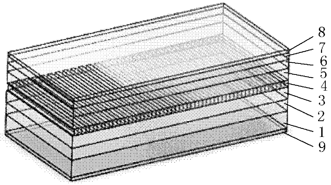
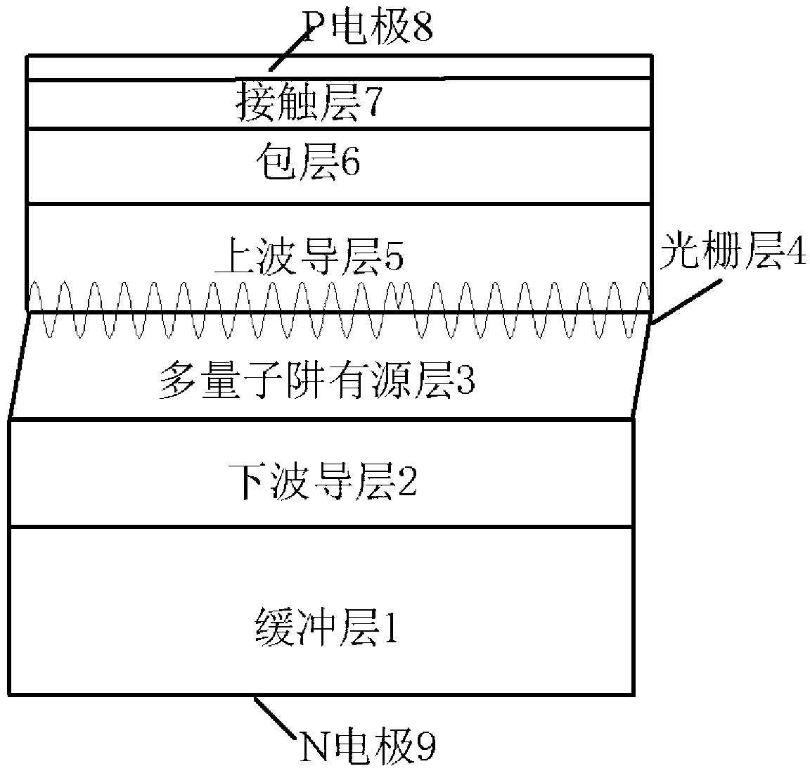
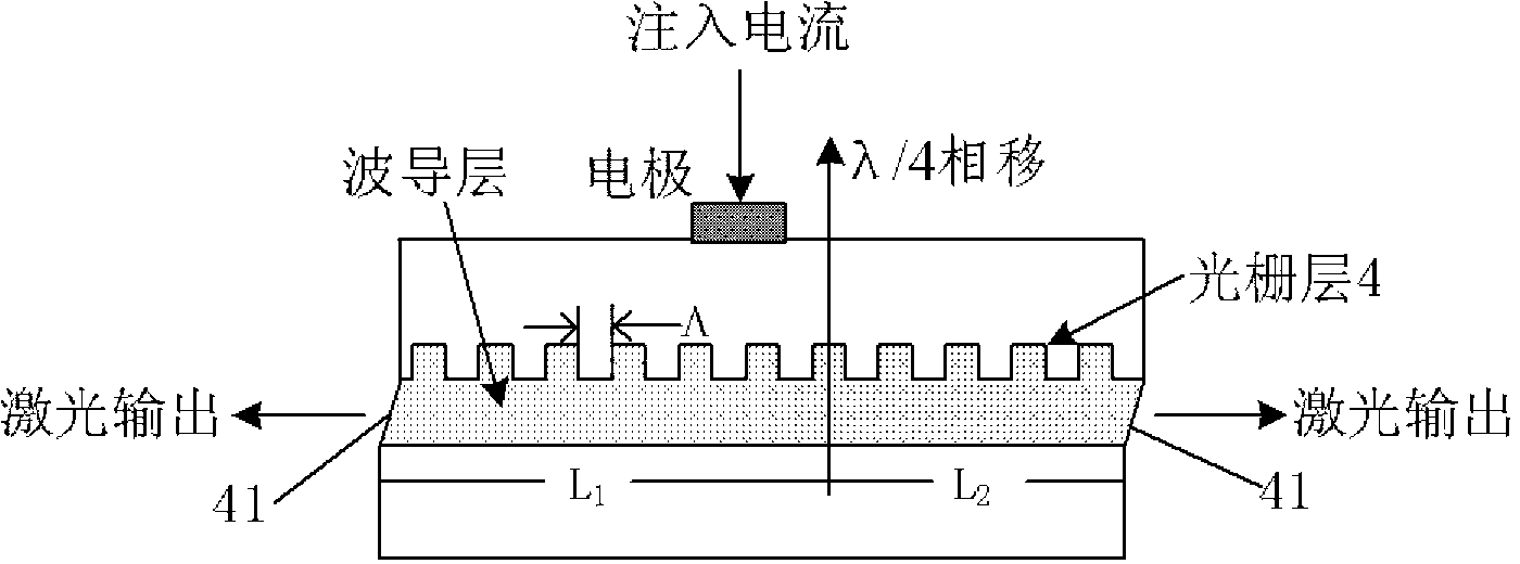
[0021] see Figure 1 to Figure 4 As shown, the present invention provides a kind of narrow-linewidth DFB semiconductor laser based on asymmetric phase-shift grating, comprising: a buffer layer 1, a lower waveguide layer 2, a multi-quantum well active layer 3, a grating layer 4, an upper A waveguide layer 5 , a cladding layer 6 , a contact layer 7 , a P electrode 8 and an N electrode 9 . in:

[0022] A buffer layer 1, the material of the buffer layer 1 is to select III-V group compound semiconductor material, II-VI group compound semiconductor material, IV-VI group compound semiconductor material or quaternary compound semiconductor material; for the InP buffer layer, the thickness is 200nm, doping concentration about 1×10 18 cm -2 .

[0023] The lower waveguide layer 2 is made on the buffer layer 1, and the thickness of the lower waveguide layer 2 is 100 nm of non-doped lattice-matched InGaAsP material.

[0024] A multi-quantum well active layer 3, the multi-quantum well ...


PUM


Abstract

The invention relates to an asymmetric phase shift grating-based narrow linewidth DFB (Described Feedback) semiconductor laser which comprises a buffer layer, a lower waveguide layer, a multiple-quantum well active layer, a grating layer, an upper waveguide layer, a package layer, a contact layer, a P electrode and an N electrode, wherein the lower waveguide layer is manufactured on the buffer layer, the multiple-quantum well active layer is manufactured on a lower package layer, the grating layer is manufactured on the multiple-quantum well active layer, the upper waveguide layer is manufactured on the grating layer, the package layer is manufactured on the upper waveguide layer, the contact layer is manufactured on the package layer, the P electrode is manufactured on the contact layer, and the N electrode is manufactured on the back surface of the buffer layer. The asymmetric phase shift grating-based narrow linewidth DFB semiconductor laser is capable of overcoming the influence of the outer reflected light to the inside of a laser device; and the laser linewidth is reduced, the frequency stability of the laser is increased and the effect of output power is improved.

Description

technical field [0001] The invention belongs to the technical field of semiconductors, in particular to a narrow line width DFB semiconductor laser based on an asymmetrical phase shift grating. Background technique [0002] Narrow linewidth semiconductor lasers have very important application value. (1) In terms of cutting-edge scientific research, it can be used in high-precision spectral measurement, quantum / atomic frequency standards and other fields; (2) In the field of national defense and security, it can be used in lidar systems, laser communications, photoelectric countermeasures, photonic navigation, etc.; (3) In the field of Internet of Things and high-speed communication, high-stability narrow-linewidth lasers are the core devices of optical fiber high-sensitivity optical fiber sensing systems and coherent optical communication systems. Compared with fiber lasers and YAG lasers, semiconductor lasers have the advantages of high reliability, long life, low energy c...

Claims


Application Information

Patent Timeline
IPC IPC(8): H01S5/12H01S5/34
Inventor 刘建国郭锦锦黄宁博孙文惠邓晔祝宁华
Owner 山东中科际联光电集成技术研究院有限公司
Why Eureka
Try Eureka