

FBAR (film bulk acoustic resonator) substrate and preparation method thereof
A thin-film bulk acoustic wave and resonator technology, applied in electrical components, impedance networks, etc., can solve problems such as damage to semiconductor chips, semiconductor CMOS process incompatibility, high substrate temperature, etc., and achieve good frequency stability.
- Summary
- Abstract
- Description
- Claims
- Application Information
AI Technical Summary
Problems solved by technology
Method used
Image

Examples
Embodiment Construction
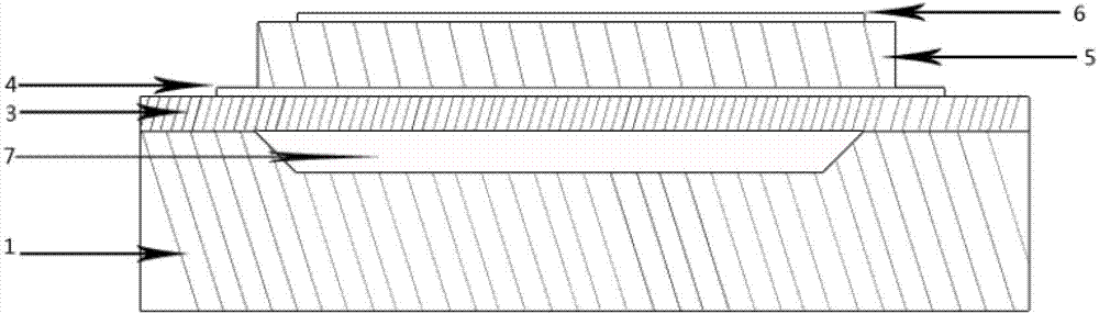
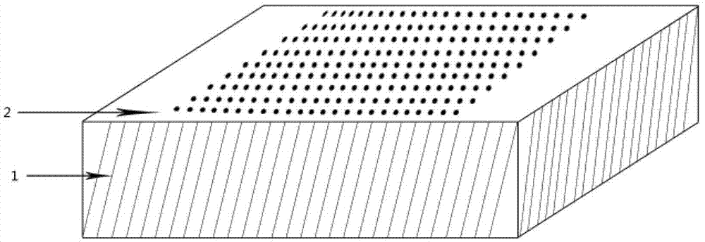
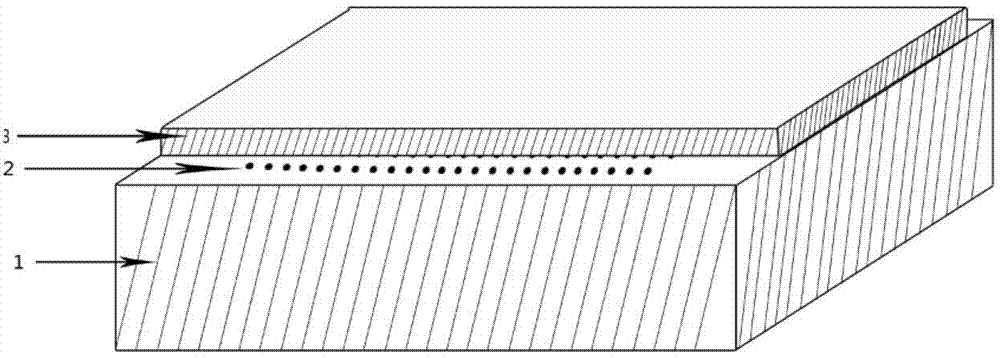
[0026] A new type of thin film bulk acoustic resonator FBAR substrate, firstly use electrochemical method to etch the selected part of Si substrate 1, that is, the air gap 7 of the mask to prepare porous silicon 2 as the air gap of the sacrificial layer; then prepare on the porous silicon The diamond-like film DLC is used as the support layer 3, and it needs to use a photoresist mask to ensure that the two sides of the diamond-like DLC film extend outside the porous silicon; the third is to prepare a W film on the DLC support layer as the bottom electrode 4; A high C-axis orientation aluminum nitride AlN piezoelectric layer 5 is prepared on the W film; the fifth is to prepare a W film on the aluminum nitride AlN piezoelectric layer as the top electrode 6; the sixth is to use the wet etching process in the IC process to etch off the porous silicon, releasing the air-gap7 structure (eg figure 1 , 4 shown).
[0027] Wherein: the surface of the silicon substrate where the porous...
PUM
 Abstract
Description
Claims
Application Information