High-transmittance photon sieve
A high transmittance, photon sieve technology, applied in the direction of diffraction grating, etc., can solve the problems of low light intensity, constant light intensity, and poor photolithography effect, so as to improve the transmittance, increase the intensity of light, and improve the quality of photolithography. effect of effect
- Summary
- Abstract
- Description
- Claims
- Application Information
AI Technical Summary
Problems solved by technology
Method used
Image

Examples
Embodiment 1
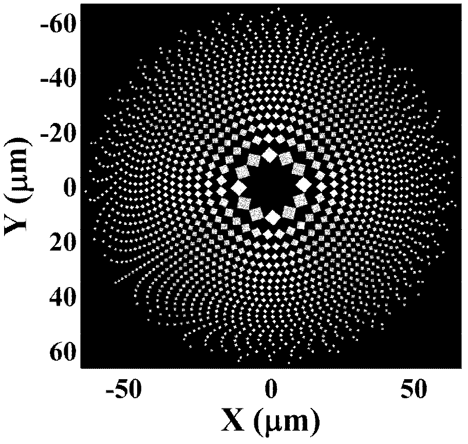
[0042] This embodiment discloses a photon sieve with high transmittance, such as figure 1 As shown, the values marked on the horizontal and vertical coordinates in the figure are the intercepted photon sieve sizes, including:
[0043] There are multiple groups of light-transmitting square microholes with different side lengths, and each group of square microholes is distributed on the same ring at intervals. The rings where each group of square microholes are located are a series of concentric circles with different radii. The radius of the mth ring is r m and belt width w m satisfy the relation:
[0044] r m 2 =2mfλ+m 2 lambda 2 ,w m = r m -r m-1 , m=1, 2, 3..., that is, m is a series of natural numbers starting from 1 and not including 0;
[0045] The λ is the wavelength of the incident light, and the f is the focal length of the photon sieve. Generally, the focal length f is fixed according to the actual situation, so the radius r of the ring can be finally dete...
Embodiment 2
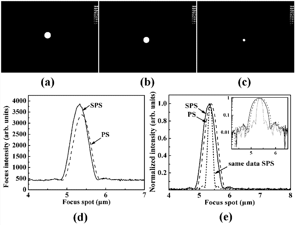
[0055] Replacing circular microholes with square microholes can increase the light intensity at the focused spot, but different effects can be achieved for different settings of square microholes. In order to achieve the best effect, this embodiment discloses an optimal high Transmittance photon sieve, the photon sieve described in this embodiment includes:
[0056] A light-transmitting quartz substrate and an opaque metal chromium film plated thereon, the diameter of the quartz substrate is 10cm, and multiple groups of light-transmitting square microholes with different side lengths are distributed on the metal chromium film. The square microholes are distributed on the same ring at intervals, the diagonal of the square microholes is parallel or perpendicular to the tangent of the ring, and the rings where each group of square microholes are located have a common center and different radii. The number m of each outer ring is a natural number selected from 1 to 370, including ...
PUM
| Property | Measurement | Unit |
|---|---|---|
| Thickness | aaaaa | aaaaa |
Abstract
Description
Claims
Application Information
 - Generate Ideas
- Intellectual Property
- Life Sciences
- Materials
- Tech Scout
- Unparalleled Data Quality
- Higher Quality Content
- 60% Fewer Hallucinations
Browse by: Latest US Patents, China's latest patents, Technical Efficacy Thesaurus, Application Domain, Technology Topic, Popular Technical Reports.
© 2025 PatSnap. All rights reserved.Legal|Privacy policy|Modern Slavery Act Transparency Statement|Sitemap|About US| Contact US: help@patsnap.com