Crystalline silicon solar cells

A technology of solar cells and crystalline silicon wafers, which is applied in the direction of circuits, electrical components, semiconductor devices, etc., can solve the problems of reducing the utilization efficiency of solar cells, high production costs of solar cells, and increased use of conductive paste, etc., to achieve increased Effects of large surface passivation area, area reduction, and print weight reduction

Active Publication Date: 2015-07-29
山东力诺阳光电力科技有限公司
View PDF4 Cites 0 Cited by
  • Summary
  • Abstract
  • Description
  • Claims
  • Application Information

AI Technical Summary

Problems solved by technology

[0004] In the prior art, solar cells adopt a structure of two main grids or three main grids, and the area covered by the main grid lines and auxiliary grid lines on the silicon wafer is relatively large, which makes the shading rate of the grid lines in the prior art reach more than 6%, reducing the The utilization efficiency of solar cells
In addition, precious metals are required as conductive paste when printing electrodes, and the large area covered by the main grid lines and sub-grid lines on the silicon wafer will inevitably increase the use of conductive paste. higher cost

Method used


Image

  • Crystalline silicon solar cells
  • Crystalline silicon solar cells
  • Crystalline silicon solar cells

Examples


Embodiment 1

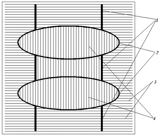
[0031] Select 156 quasi-monocrystalline silicon wafer cells, the front grid line structure includes: first-level main grid 1, second-level main grid 2 and auxiliary grid; among them, there are two first-level main grids 1 parallel to each other, and each first-level main grid 1 is divided into three sections, the second-level main grid 2 connects the segments of the first-level main grid 1 in sequence and forms two ovals, the first-level auxiliary grid 3 is perpendicular to the first-level main grid 1 and connected together and is located on the second-level main grid In addition to the pattern of the grid 2, the second-level sub-gate 4 is parallel to the first-level main grid 1 and is located within the graphics of the second-level main grid 2 and connected to the second-level main grid; the width of the second-level main grid ≤ the first-level main grid width. There are two electrodes on the back, and the shape and structure correspond to the first-level busbar 1 on the fron...

Embodiment 2

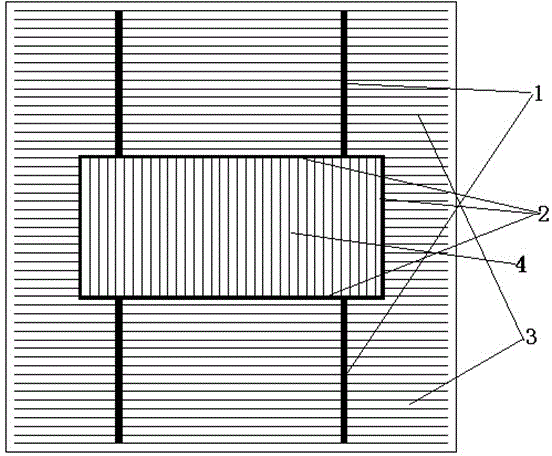
[0033] Select 125 monocrystalline silicon wafer cells, the front grid line structure includes: first-level main grid 1, second-level main grid 2 and auxiliary grid; among them, there are two first-level main grids 1 parallel to each other, and each first-level main grid 1 Divided into two sections, the second-level main grid 2 is square and connects the first-level main grid 1 segmentally, the first-level auxiliary grid 3 is perpendicular to the first-level main grid 1 and connected together, and is located between the graphics of the second-level main grid 2 In addition, the secondary sub-gate 4 is parallel to the primary main gate 1 within the pattern of the secondary main gate 2 and connected to the secondary main gate; the width of the secondary main gate ≤ the width of the primary main gate. There are two electrodes on the back, and the shape and structure correspond to the first-level busbar 1 on the front.

Embodiment 3

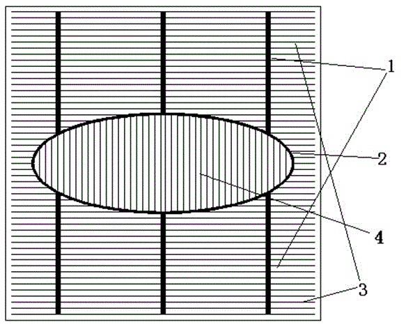
[0035] Select 156 monocrystalline silicon wafer cells, the front grid line structure includes: first-level main grid 1, second-level main grid 2 and auxiliary grid; among them, the first-level main grid 1 consists of two parallel to each other, and each first-level main grid 1 Set in two sections, the secondary main grid 2 is elliptical and connects the first-level main grid 1 in sections, the first-level sub-grid 3 is perpendicular to the first-level main grid 1 and connected together, and is located in the figure of the second-level main grid 2 In addition, the secondary sub-gate 4 is parallel to the primary main gate 1 within the pattern of the secondary main gate 2 and connected to the secondary main gate; the width of the secondary main gate ≤ the width of the primary main gate. There are three electrodes on the back, and the shape and structure correspond to the first-level main grid 1 on the front.


PUM


Abstract

The invention relates to a silicon solar battery piece which comprises a crystal silicon slice, a front face grid line and a back face electrode. The front face grid line is located on the illuminated face of a battery and comprises a main grid and a vice grid. The main grid comprises primary main grids and secondary main grids, wherein the number of the primary main grids is at least two, the primary main grids are mutually parallel, each primary main grid is divided into at least two sections, and the secondary main grids are connected at the positions of fractured openings of the primary main grids through regular or irregular shapes or lines. The vice grid comprises primary vice grids and secondary vice grids, wherein the primary vice grids are evenly distributed outside the shapes which are formed by the secondary main grids and are perpendicular to the primary main grids, and the secondary vice grids are located inside the shapes which are formed by the secondary main grids and are arranged parallel to the primary main grids. On one hand, direct contact of a main gate electrode and the silicon slice can be decreased, surface passivation area is enlarged, the illuminated area of the solar battery is increased, and the photoelectric conversion efficiency of the solar battery is effectively improved; and on the other hand, silver paste consumption in the manufacturing process can be effectively reduced, and production cost is lowered.

Description

technical field [0001] The invention relates to a solar cell, in particular to a crystalline silicon solar cell. Background technique [0002] The rapid development of the solar energy industry needs to continuously reduce the cost of materials, improve the efficiency of photoelectric conversion to reduce the cost of power generation, and achieve the goal of being the same price as the mains electricity or lower than the price of the mains electricity. [0003] With the development of industrialization, conventional crystalline silicon cells have made great progress in improving conversion efficiency and reducing costs. The manufacturing process of crystalline silicon solar cells generally has the following steps: chemical cleaning and surface texture treatment, diffusion junction, edge etching and phosphorus silicon glass removal, anti-reflection film deposition, electrode printing, and sintering. In the process of converting light energy into electrical energy in a solar ...

Claims


Application Information

Patent Timeline
Patent Type & Authority Patents(China)
IPC IPC(8): H01L31/0224
Inventor 任现坤张春艳贾河顺马继磊程亮徐振华姜言森孙继峰
Owner 山东力诺阳光电力科技有限公司
Why Eureka
Try Eureka