Cu2ZnSnS4/a-Si heterojunction solar cell and manufacturing method thereof

A technology of solar cells and heterojunctions, applied in circuits, photovoltaic power generation, electrical components, etc., can solve problems such as battery environmental pollution

Inactive Publication Date: 2013-05-08
NANJING UNIV OF AERONAUTICS & ASTRONAUTICS
View PDF5 Cites 6 Cited by
  • Summary
  • Abstract
  • Description
  • Claims
  • Application Information

AI Technical Summary

Problems solved by technology

It is mainly summarized as a heterojunction battery of CZTS and CdS, but Cd is toxic, so this...

Method used


Image

  • Cu2ZnSnS4/a-Si heterojunction solar cell and manufacturing method thereof
  • Cu2ZnSnS4/a-Si heterojunction solar cell and manufacturing method thereof
  • Cu2ZnSnS4/a-Si heterojunction solar cell and manufacturing method thereof

Examples


preparation example Construction

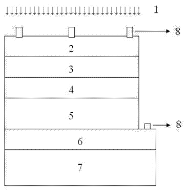
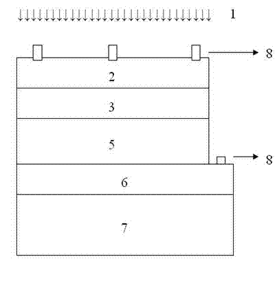
[0022] The above Cu-based 2 ZnSnS 4 Novel Cu for Heterojunction Solar Cells 2 ZnSnS 4 A method for preparing an α-Si heterojunction solar cell, characterized in that it comprises the following preparation steps:

[0023] Step 1. The substrate is cleaned, and the substrate in the tool is selected from FTO glass or metal sheet or metal-coated glass substrate;

[0024] Step 2, preparation of CZTS thin film: using magnetron sputtering metal multilayer film preset layer subsequent vulcanization method to prepare p-type CZTS thin film,

[0025] This step can adopt existing technology, concrete steps are as follows:

[0026] (2-1) First, the magnetron sputtering method is used to sputter Zn, Sn and Cu films on the substrate in turn (the sequence can be adjusted), wherein the purity of each metal target is higher than 99.999%; wherein each layer of metal Thin film sputtering parameters: the background vacuum is 5*10 -2 pa-5*10 -4 pa, the Ar flow rate is 5sccm-100sccm, the sputt...

specific example 1

[0033] The present invention will be further described below in conjunction with the examples, but the protection scope of the present invention should not be limited thereby.

[0034] A new type of Cu 2 ZnSnS 4 A thin-film solar cell and a preparation method thereof, comprising the steps of:

[0035] (1) Clean the ordinary FTO glass substrate, the specific process is as follows:

[0036] Organic solvent ultrasonic cleaning → acetone ultrasonic cleaning → alcohol ultrasonic cleaning → ultrapure water ultrasonic cleaning

[0037] (2) Sputtering Zn, Sn and Cu films respectively in sequence on the above-mentioned cleaned FTO substrate. The corresponding metal thin film sputtering parameters of each layer are as follows:

[0038] Zn film sputtering parameters: the background vacuum is 5*10 -4 pa, the Ar flow rate is 20sccm, the sputtering pressure is kept constant at 0.1pa, the sputtering power is 20W, and the sputtering thickness is 60nm.

[0039] Sn film sputtering paramet...

specific example 2

[0050] The present invention will be further described below in conjunction with the examples, but the protection scope of the present invention should not be limited thereby.

[0051] A new type of Cu 2 ZnSnS 4 A thin-film solar cell and a preparation method thereof, comprising the steps of:

[0052] (1) Clean the ordinary FTO glass substrate, the specific process is as follows:

[0053] Organic solvent ultrasonic cleaning → acetone ultrasonic cleaning → alcohol ultrasonic cleaning → ultrapure water ultrasonic cleaning

[0054] (2) Sn, Zn and Cu films were respectively sputtered successively on the above-mentioned cleaned FTO substrate. The corresponding metal thin film sputtering parameters of each layer are as follows:

[0055] Sn film sputtering parameters: the background vacuum is 5*10 -4 pa, the Ar flow rate is 20 sccm, the sputtering pressure is kept constant at 0.1 Pa, the sputtering power is 30 W, the sputtering film thickness is 140 nm, and the substrate tempera...


PUM

PropertyMeasurementUnit
Thicknessaaaaaaaaaa
Thicknessaaaaaaaaaa
Absorption coefficientaaaaaaaaaa

Abstract

The invention discloses a Cu2ZnSnS4/a-Si heterojunction solar cell and a manufacturing method thereof, and belongs to the technical field of solar cell device design and novel materials. The solar cell has two structures, wherein the first structure is a heterogeneous p-i-n junction composed of a p-type layer, an i-type layer and an n-type layer, the p-type layer is copper zinc tin sulfide (CZTS), and the first structure is characterized in that the i-type layer and the n-type layer are both alpha-Si, and a transparent conductive electrode is deposited on the n-type layer. The second structure is a heterogeneous p-n junction composed of the i-type layer and the n-type layer, the p-type layer is CZTS, and the second structure is characterized in that the n-type layer is alpha-Si, and a transparent conductive electrode is deposited on the n-type layer. The solar cell is novel in structure, completely free of poison and low in price, and has wide application prospect and large commercial value.

Description

technical field [0001] The invention relates to a Cu-based 2 ZnSnS 4 (CZTS)Cu 2 ZnSnS 4 The invention relates to an α-Si heterojunction solar cell and a preparation method thereof, which belong to the technical field of new materials and new structures of solar cell devices. Background technique [0002] Global energy shortages, environmental pollution, and climate warming are increasingly plaguing human society. Seeking green alternative energy to achieve sustainable development has become a common issue faced by all countries in the world. In the long run, renewable energy will be the main source of energy for human beings in the future. In the use of newly developed renewable energy, solar cells have the most potential. [0003] However, due to the shortage of silicon materials in the world and the high production cost, thin-film solar cells have attracted widespread attention, and have become the research focus of scientific and technological workers in recent year...

Claims


Application Information

Patent Timeline
IPC IPC(8): H01L31/032H01L31/0392H01L31/075H01L31/074H01L31/20
CPCY02E10/50Y02E10/548Y02P70/50
Inventor 沈鸿烈江丰王威张磊
Owner NANJING UNIV OF AERONAUTICS & ASTRONAUTICS
Why Eureka
Try Eureka