Novel light emitting diode based on photonic crystal

A technology of light-emitting diodes and photonic crystals, which is applied in the direction of semiconductor devices, electrical components, circuits, etc., can solve the problems of unsatisfactory light output effects of light-emitting diodes, not suitable for low-cost mass production, high design costs, etc., and achieve the improvement of luminous efficiency , easy processing, convenient processing effect

Inactive Publication Date: 2013-05-08
HENAN UNIV OF SCI & TECH
View PDF6 Cites 1 Cited by
  • Summary
  • Abstract
  • Description
  • Claims
  • Application Information

AI Technical Summary

Problems solved by technology

[0004] The traditional methods to improve LED include adopting an inverted pyramid structure, adding a reflective layer and a roughened film structure, etc., all of which can improve the luminous efficiency of the LED to a certain extent, but due to poor packaging, complicated process, and design The cost is too high and the effect of improving the light output of LEDs is not ideal, so it is not suitable for low-cost mass production

Method used


Image

  • Novel light emitting diode based on photonic crystal
  • Novel light emitting diode based on photonic crystal
  • Novel light emitting diode based on photonic crystal

Examples


Embodiment Construction

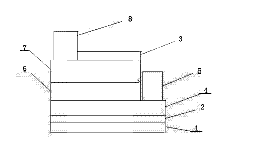
[0033] As shown in the figure, a new light-emitting diode based on photonic crystals is provided with an LED chip. The LED chip includes a substrate 1, a first surface layer 2, a second surface layer 3 and a light-emitting crystal layer. The light-emitting crystal layer consists of an N-type Material layer 4, N-type electrode layer 5, active layer 6, P-type material layer 7 and P-type electrode layer 8, the first surface layer 2 and the second surface layer 3 are photonic crystals, the photonic crystals of the two surface layers The structure is the same, the base material 1 is provided with a first surface layer 2, and an N-type material layer 4, an N-type electrode layer 5, an active layer 6, a P-type material layer 7, and a P-type electrode layer are sequentially added on the first surface layer 2. Layer 8 and the second surface layer 3, the second surface layer 3 is arranged on one side of the P-type electrode layer 8, on the P-type electrode layer 8 and the N-type electrod...


PUM


Abstract

A novel light emitting diode based on a photonic crystal is provided with a light-emitting diode (LED) chip which comprises base materials, a first surface layer, a second surface layer and a luminescence crystal layer. The luminescence crystal layer comprises an N type material layer, an N type electrode layer, an active layer, a P type material layer and a P type electrode layer. Photonic band gap properties of the photonic crystal are utilized, namely when light with frequency in the range of photonic band gap frequency enters the photonic crystal, incident waves can be completely reflected back due to that the photonic crystal has no corresponding transmission mode with a photonic band gap. The photonic crystal can be added into an ordinary LED, the light which is refracted and absorbed and the like in the LED and can not be transferred outside can be completely reflected and become the light capable of being transferred out of a light body and being used by people, and therefore utilization efficiency of a luminescence power source is improved.

Description

technical field [0001] The invention relates to the technical field of one-dimensional photonic crystals, in particular to a novel light-emitting diode based on photonic crystals. Background technique [0002] Light-emitting diode (LED) is an electroluminescent optoelectronic device, and its application is of great significance to the energy development of society. It has been more than 30 years since its initial discovery and production. It is a solid-state light source that is gradually developing and has been widely used. Nowadays, various types of LEDs, products using LEDs for secondary development, and products matching LEDs (such as white light LED drivers) are developing rapidly, and new products are constantly on the market, which has developed into many new industries. LED has many advantages such as long life, high reliability, environmental protection, and small size. It is called the third-generation lighting source after incandescent lamps and fluorescent lamps...

Claims


Application Information

Patent Timeline
Patent Type & Authority Applications(China)
IPC IPC(8): H01L33/10H01L33/46
Inventor 李萍韩志中张兰兰梁高峰雷茂生赵新峰张霞赵彬姜婷宋霄薇蔺利峰乔晓岚
Owner HENAN UNIV OF SCI & TECH
Why Eureka
Try Eureka