Clock synchronous device and system for Field Programmable Gate Array (FPGA) prototype test plate piling

A prototype verification and clock synchronization technology, applied in the field of FPGA prototype verification, can solve the problems of unguaranteed quality and difficulty in flexible change of the number of synchronization clocks, to simplify the circuit design structure, improve the clock synchronization efficiency, improve the clock synchronization efficiency and The effect of precision

Active Publication Date: 2013-05-15
杭州乔微电子科技有限公司
View PDF4 Cites 22 Cited by
  • Summary
  • Abstract
  • Description
  • Claims
  • Application Information

AI Technical Summary

Problems solved by technology

This method is not only limited by a single crystal oscillator or a single programmable clock shared pin, but also affected by the qual

Method used


Image

  • Clock synchronous device and system for Field Programmable Gate Array (FPGA) prototype test plate piling
  • Clock synchronous device and system for Field Programmable Gate Array (FPGA) prototype test plate piling

Examples


Embodiment Construction

[0029] In order to make the object, technical solution and advantages of the present invention clearer, the present invention will be further described in detail below in conjunction with the accompanying drawings and embodiments. It should be understood that the specific embodiments described here are only used to explain the present invention, not to limit the present invention.

[0030] On the contrary, the invention covers any alternatives, modifications, equivalent methods and schemes within the spirit and scope of the invention as defined by the claims. Further, in order to make the public have a better understanding of the present invention, some specific details are described in detail in the detailed description of the present invention below. The present invention can be fully understood by those skilled in the art without the description of these detailed parts.

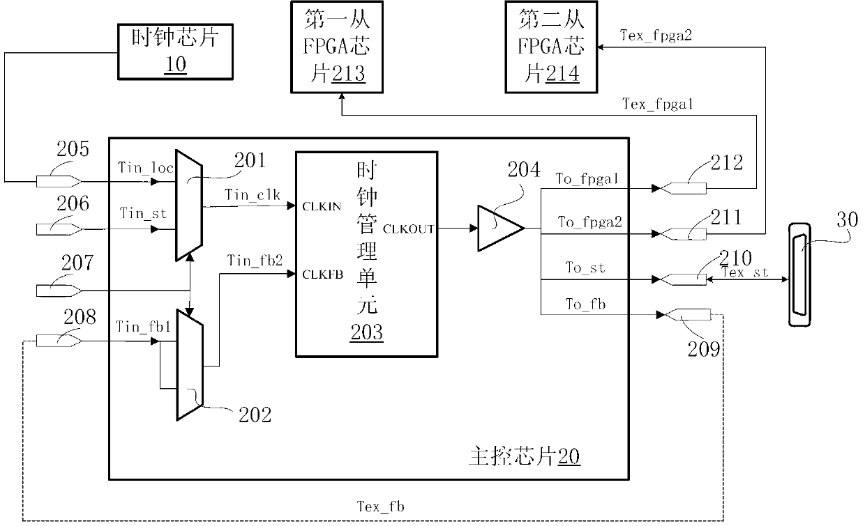
[0031] refer to figure 1 , which shows the principle structure diagram of the clock synchronization d...


PUM


Abstract

The invention discloses a clock synchronous device and a system for Field Programmable Gate Array (FPGA) prototype test plate piling, wherein the clock synchronous device for FPGA prototype test plate piling comprises a clock chip, a master control chip, at least one slave FPGA chip and at least one high-speed connector, wherein the main control chip further comprises a first data selector, a second data selector, a clock management unit and a global clock buffer. The master chip comprises a local clock input pin, a piling clock input pin, a selective signal input pin, a selective signal input pin, a feedback clock input pin, a slave FPGA clock synchronization clock signal output pin, a feedback clock synchronization clock signal output pin and a high-speed connector synchronization clock signal output pin. The clock synchronous device and the system for FPGA prototype test plate piling utilize a master control chip inner lock phrase loop to feed back, the time delay of a master control chip inner routing is equal to the corresponding routing time delay of an outer PCB plate, and the clocks which are output to all slave FPGA chip are enabled to achieve synchronization.

Description

technical field [0001] The invention belongs to the technical field of FPGA prototype verification, and in particular relates to a clock synchronization device and system for stacking FPGA prototype verification boards. Background technique [0002] Field Programmable Gate Array (Field Program Gate Array, FPGA) prototype verification is a methodology for building a prototype of a System on Chip (System on Chip, SOC) and an Application Specific Integrated Circuit (ASIC) on an FPGA. Convenient hardware verification and early software development, this methodology is also called ASIC prototype verification or SOC prototype verification, which can speed up the development of ASIC and other designs, shorten the development cycle, reduce the development cost of ASIC application systems, and improve the success of tape-out Rate. [0003] In the field of FPGA prototype verification, when the capacity of FPGA logic gates on a single board does not meet the user's logic requirements,...

Claims


Application Information

Patent Timeline
IPC IPC(8): G06F1/12G06F11/26
Inventor 郑利浩
Owner 杭州乔微电子科技有限公司
Why Eureka
Try Eureka