
Substrate processing apparatus

A substrate processing device and processing device technology, applied in the direction of gaseous chemical plating, coating, electrical components, etc., can solve the problems of long path, large power loss, poor matching, etc., and achieve suppressed power loss, small fluctuation rate, The effect of small current difference

Inactive Publication Date: 2013-05-15
TOKYO ELECTRON LTD
View PDF5 Cites 6 Cited by
  • Summary
  • Abstract
  • Description
  • Claims
  • Application Information

AI Technical Summary

Problems solved by technology

However, these techniques are not techniques for solving the above-mentioned problems caused by the small output impedance of the matcher, and such problems still exist even if these techniques are applied.
In addition, in the case of supplying power to both sides of the electrode through the matching unit, the two matching units are connected to the same load, so there is a problem of poor matching caused by mutual interference, and two expensive high-current The number of matching devices for variable capacitors increases, so the device cost becomes higher
In addition, when the output of the low-impedance matching device is branched and connected to both sides of the electrode, the path through which the high-power high-frequency power flows becomes long, and the power loss is extremely large.

Method used


Image

  • Substrate processing apparatus
  • Substrate processing apparatus
  • Substrate processing apparatus

Examples


no. 1 approach )

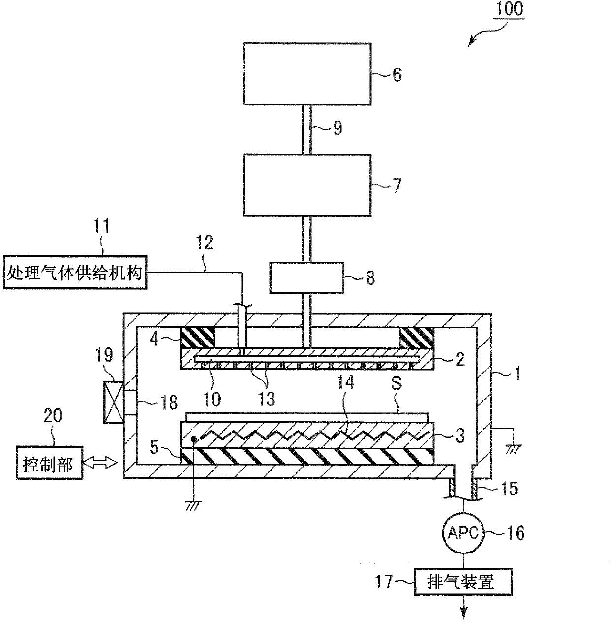
[0051] First, a first embodiment will be described. figure 1 It is a sectional view showing the substrate processing apparatus according to the first embodiment of the present invention.

[0052] The substrate processing apparatus 100 is configured as a parallel plate type plasma processing apparatus that performs plasma processing on a substrate. This substrate processing apparatus 100 accommodates a substrate S and has a chamber 1 for performing plasma processing. Chamber 1 is safely grounded.

[0053] A cathode electrode 2 and an anode electrode 3 constituting parallel plate electrodes are arranged in the chamber 1 . The cathode electrode 2 is configured as an upper electrode, and functions as a plasma generation electrode supplied with high-frequency power. In addition, the cathode electrode 2 functions as a shower head for introducing process gas into the chamber 1 . On the other hand, the anode electrode 3 is configured as a lower electrode, and functions as a mounti...

no. 2 approach )

[0070] Next, a second embodiment will be described. Figure 4 It is a schematic diagram showing the substrate processing apparatus of the second embodiment. The basic structure of the substrate processing apparatus 100 ′ of this embodiment is the same as that of the substrate processing apparatus 100 of the first embodiment. Figure 4 right with figure 1 The same reference numerals are assigned to the same parts, and explanations thereof are omitted.

[0071] This embodiment differs from the first embodiment in that two impedance adjustment circuits 8a, 8b are provided, and power is supplied from mutually opposing feeding points on both sides of the cathode electrode via these impedance adjustment circuits 8a, 8b.

[0072] Specifically, the transmission path 9 extending downward from the matching unit 7 is branched into the transmission paths 9a and 9b, and connected to the power supply points on both sides of the cathode electrode 2 facing each other, and impedances are res...

no. 3 approach )

[0078] Next, a third embodiment will be described. Figure 5 It is a schematic diagram showing the substrate processing apparatus of the third embodiment. The substrate processing apparatus 200 of the present embodiment is basically a substrate processing apparatus in which the substrate processing apparatus 100 of the first embodiment is applied to an apparatus (batch type apparatus) that performs plasma processing on a plurality of substrates. Thus, in Figure 5 In the pair with figure 1 The parts with the same functions are denoted by the same reference numerals for description.

[0079] The substrate processing apparatus 200 is configured as a parallel plate type plasma processing apparatus for performing plasma processing on a plurality of substrates, and accommodates a plurality (in Figure 5 There are three substrates S with a chamber 1 for plasma processing. The chamber 1 is safely grounded as in the first embodiment.

[0080] In the chamber 1, a plurality of pair...


PUM


Abstract

A substrate processing apparatus 100 includes a high frequency power supply configured to generate a high frequency power 6; a plasma generation electrode 2 configured to generate the plasma by the high frequency power 6 supplied from the high frequency power supply; a single matching unit 7 provided between the high frequency power supply 6 and the plasma generation electrode 2, and configured to match an impedance of a transmission path 9 and an impedance of a load; and an impedance adjusting circuit 8 provided between the matching unit 7 and the plasma generation electrode 2, and configured to adjust an impedance therebetween. The matching unit 7 performs impedance matching by setting the plasma and the impedance adjusting circuit 8 as a single load, and an output impedance of the matching unit is adjusted to a value higher than an impedance of the plasma by adjusting the impedance by the impedance adjusting circuit 8.

Description

technical field [0001] The present invention relates to a substrate processing apparatus configured as a parallel plate type plasma processing apparatus. Background technique [0002] At present, as a parallel plate type plasma processing device, there is known a device in which an anode and a cathode electrode are provided in a chamber, and a high-frequency power is supplied to the cathode electrode from a power supply provided outside the chamber through a matcher (for example, patent Literature 1). [0003] Usually, the impedance of the plasma load is about 1 to several Ω, and therefore, the matching unit needs to match 50Ω, which is the impedance of the transmission path, with a low impedance of about 1 to several Ω. [0004] When applying such a parallel plate type plasma processing apparatus to plasma processing of large substrates used in solar cell panels or flat panel panels, a large power is required, and, as described above, it is necessary to achieve a low imped...

Claims


Application Information

Patent Timeline
Patent Type & Authority Applications(China)
IPC IPC(8): H01J37/32H01J37/24
CPCH01J37/32091H01J37/32183
Inventor 花轮健一
Owner TOKYO ELECTRON LTD
Learn More