Atomic layer deposition equipment

A technology of atomic layer deposition and equipment, which is applied in the direction of coating, metal material coating process, gaseous chemical plating, etc., can solve the problems that the processing cycle cannot be shortened and the growth efficiency is low

Inactive Publication Date: 2013-05-22
INST OF SEMICONDUCTORS - CHINESE ACAD OF SCI
View PDF2 Cites 6 Cited by
  • Summary
  • Abstract
  • Description
  • Claims
  • Application Information

AI Technical Summary

Problems solved by technology

In the above process, it takes 10 to 100 seconds to evacuate according to the size of the reaction chamber, and only two atomic layers can be grown in each reaction c

Method used


Image

  • Atomic layer deposition equipment
  • Atomic layer deposition equipment
  • Atomic layer deposition equipment

Examples


Embodiment Construction

[0012] In order to make the object, technical solution and advantages of the present invention clearer, the present invention will be described in further detail below in conjunction with specific embodiments and with reference to the accompanying drawings.

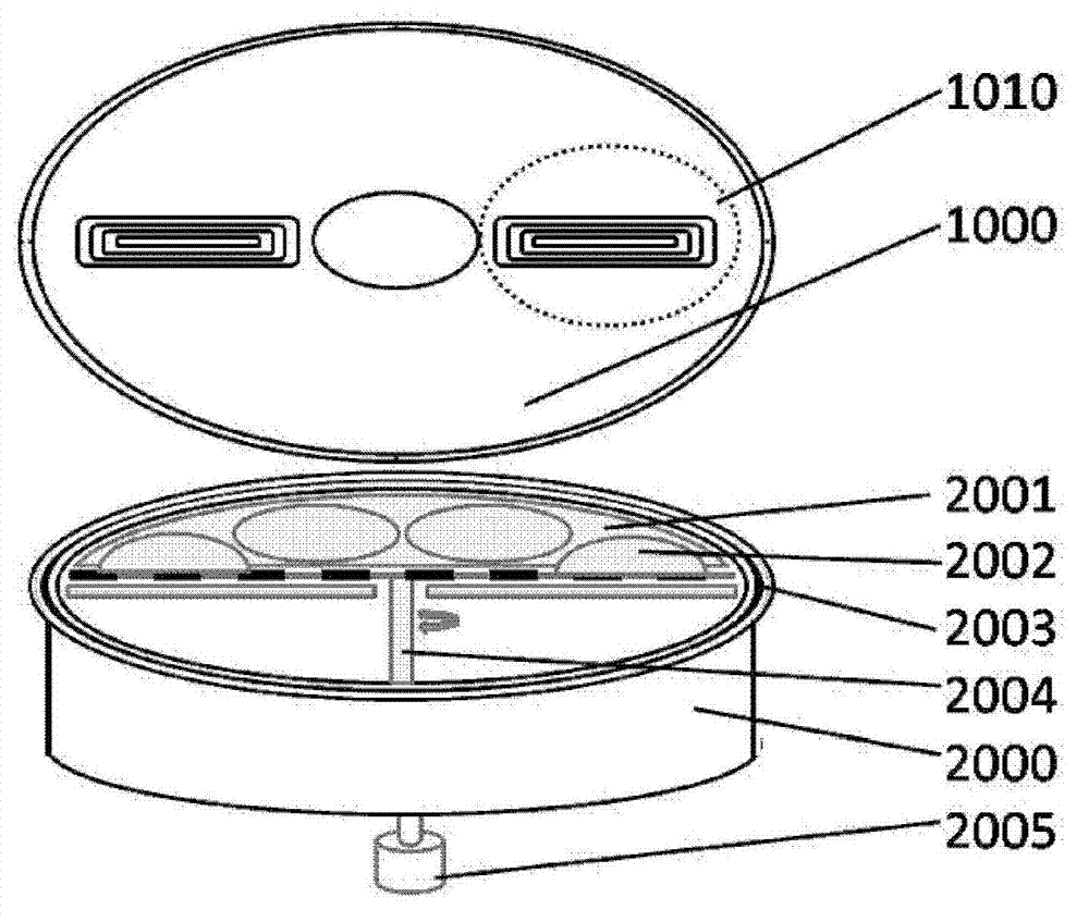
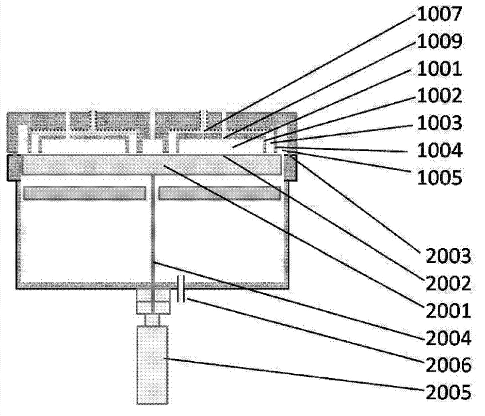
[0013] Such as figure 1 As shown, the present invention proposes an atomic layer deposition equipment, which is an openable and closed closed chamber composed of a cover plate 1000 and a main chamber 2000; wherein the inner surface of the cover plate 1000 is provided with a gas path unit 1010 ; The main chamber has a rotating system 2005, a rotating bearing plate 2001 and a sealing rubber ring 2003.

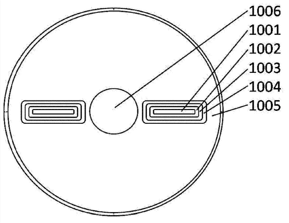
[0014] In a preferred embodiment of the present invention, as figure 1 and Figure 5 As shown, the cover plate 1000 has two sets of air path units 1010, the two sets of air path units are symmetrically distributed about the geometric center of the cover plate, and each set of air path units has two air flow channels, that ...


PUM


Abstract

The invention discloses atomic layer deposition equipment which is an openable and closable closed cavity comprising a cover plate and a main cavity, wherein the inner surface of the cover plate is provided with an air path unit; the air path unit comprises a plurality of airflow channels; the plurality of airflow channels are spaced through spacing layers, and each airflow channel is communicated with a plurality of air holes arranged on the outer surface of the cover plate; the main cavity comprises a rotatable loading disc and a transmission system; the transmission system drives the rotatable loading disc to rotate; the rotatable loading disc is provided with a groove used for placing a wafer; the plurality of airflow channels at least include a first airflow channel and a second airflow channel; the first airflow channel is used for accessing a reaction source gas; and the second airflow channel is used for exhausting the unreacted reaction source gas. The atomic layer deposition equipment disclosed by the invention can increase the speed of atomic layer epitaxy, save the single process time and enhance the growth rate of the atomic layer epitaxy by increasing the rotation speed of the loading disc.

Description

technical field [0001] The invention relates to the field of manufacturing microelectronic devices, in particular to an atomic layer deposition (ALD) device. Background technique [0002] Atomic layer deposition (ALD) is a method that can deposit thin films layer by layer in the form of single atomic layers on the surface of a substrate. Atomic layer deposition is similar to ordinary chemical deposition. But in ALD, the chemical reaction of a new atomic film is directly linked to the previous one, in such a way that only one layer of atoms is deposited per reaction. [0003] Atomic layer deposition (ALD) technology is gradually becoming a necessary technology in the field of microelectronic device manufacturing, such as for the preparation of high-k dielectric and metal films, copper barrier / seed films, etch stop layers in transistor gate stacks and capacitors , a variety of gap layers and thin-film diffusion barriers, magnetic heads, and non-volatile memories. ALD has in...

Claims


Application Information

Patent Timeline
IPC IPC(8): C23C16/455
Inventor 赵万顺张峰王雷曾一平
Owner INST OF SEMICONDUCTORS - CHINESE ACAD OF SCI
Why Eureka
Try Eureka