Pixel structure and method for manufacturing the same

A technology of pixel structure and fabrication method, applied in semiconductor/solid-state device fabrication, electrical components, transistors, etc., can solve the problems of difficult electrical connection of pixel electrodes, lowering of display yield, etc.

Inactive Publication Date: 2013-05-29
AU OPTRONICS CORP
View PDF2 Cites 15 Cited by
  • Summary
  • Abstract
  • Description
  • Claims
  • Application Information

AI Technical Summary

Problems solved by technology

However, the arrangement of such a thick planar layer often results in its front and rear layers, for example, the pixel electrodes formed behind and above the planar layer are not easily electrically connected to the drains formed before and below the planar layer. electrode, which reduces the yield of the display

Method used


Image

  • Pixel structure and method for manufacturing the same
  • Pixel structure and method for manufacturing the same
  • Pixel structure and method for manufacturing the same

Examples


Embodiment Construction

[0027] In order to enable those who are familiar with the technical field of the present invention to have a better understanding of the present invention, the following special publications cite the preferred embodiments of the present invention and, in conjunction with the accompanying drawings, describe in detail the content of the present invention and the effects to be achieved. .

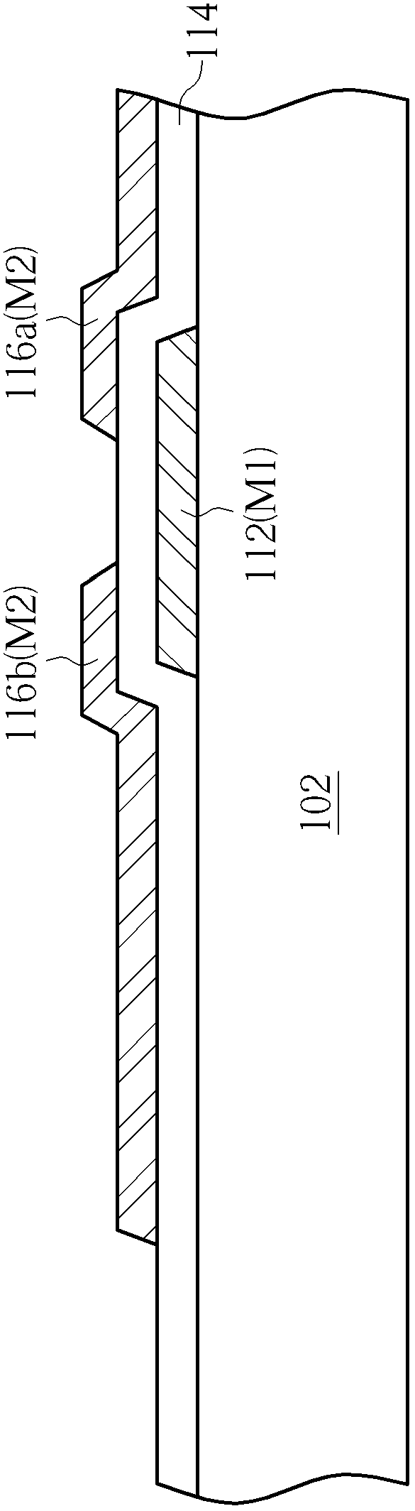
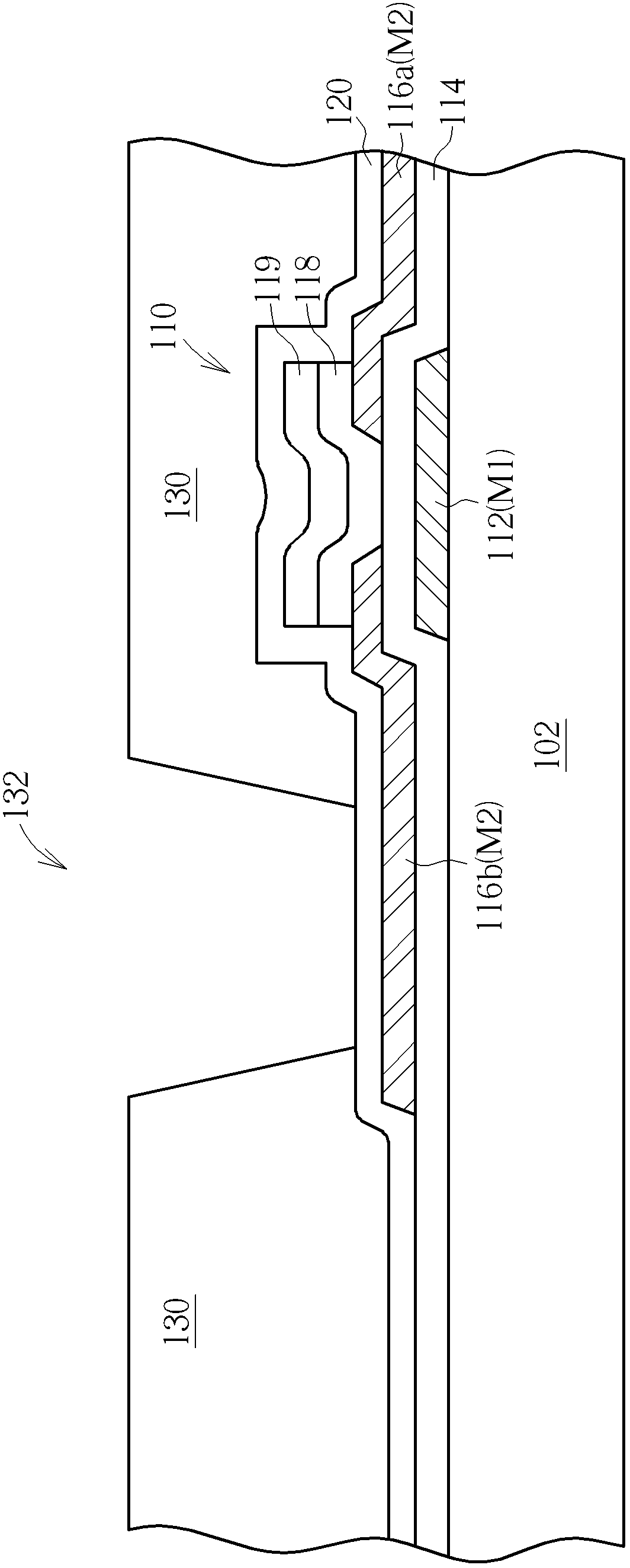
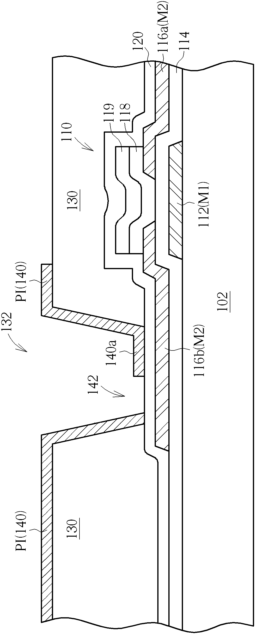
[0028] Please refer to Figure 1 to Figure 9 ,among them Figure 1 to Figure 7 A schematic diagram of a method for manufacturing a pixel structure provided by a preferred embodiment of the present invention is shown, Figure 8 Is a schematic diagram of a pixel structure provided by this preferred embodiment, and Picture 9 It is a partially enlarged schematic diagram of the pixel structure. Such as figure 1 As shown, first, a substrate 102 is provided. The substrate 102 can be a rigid substrate such as a glass substrate, or a flexible substrate such as a plastic substrate, but is not limited to t...


PUM


Abstract

The invention relates to a pixel structure and a method for manufacturing the same. The manufacture method comprises the following steps of providing a substrate; forming a thin film transistor, a first protection layer, a flat layer possessing a first opening, a patterned first conductive layer possessing a second opening, a second protection layer and a light resistance pattern layer on the substrate; via the light resistance pattern layer, etching the second protection layer to form a third opening exposed out of a part of the patterned first conductive layer and a part of the first protection layer; via the patterned first conductive layer, etching the first protection layer to form a fourth opening exposed out of a part of a drain electrode of the thin film transistor; removing the light resistance pattern layer; and forming patterned second conductive layers of the patterned first conductive layer and the drain electrode electrically connected in the second, third and fourth openings and on the second protection layer.

Description

Technical field [0001] The present invention relates to a pixel structure and a manufacturing method thereof, in particular to a high-resolution pixel structure and a manufacturing method thereof. Background technique [0002] Flat-panel displays, such as liquid crystal displays, have replaced traditional cathode ray tube (CRT) displays and have become the mainstream of displays due to their characteristics of lightness, thinness, short size, low radiation, and low power consumption. In the development of the display, it is constantly moving in the direction of high-resolution requirements. However, with the increase in resolution, the number of thin film transistors (TFT) on the panel has also increased, resulting in the continuous reduction of the available space on the panel. At the same time, in order to improve the aperture ratio and the performance of thin film transistors, the number of photo-etching processes (hereinafter referred to as PEP) has been increased in the pro...

Claims


Application Information

Patent Timeline
Patent Type & Authority Applications(China)
IPC IPC(8): H01L21/77H01L27/02H01L29/786
Inventor 张玮伦黄国有陈勃学
Owner AU OPTRONICS CORP
Why Eureka
Try Eureka