Thin film transistor liquid crystal display (LCD) array substrate
A liquid crystal display and thin film transistor technology, applied in the field of liquid crystal display, can solve the problems of high occurrence rate of flicker and crosstalk, and achieve the effect of reducing resistance, reducing delay time, and reducing the incidence of undesirable phenomena such as flicker and crosstalk
- Summary
- Abstract
- Description
- Claims
- Application Information
AI Technical Summary
Problems solved by technology
Method used
Image

Examples
Embodiment 1
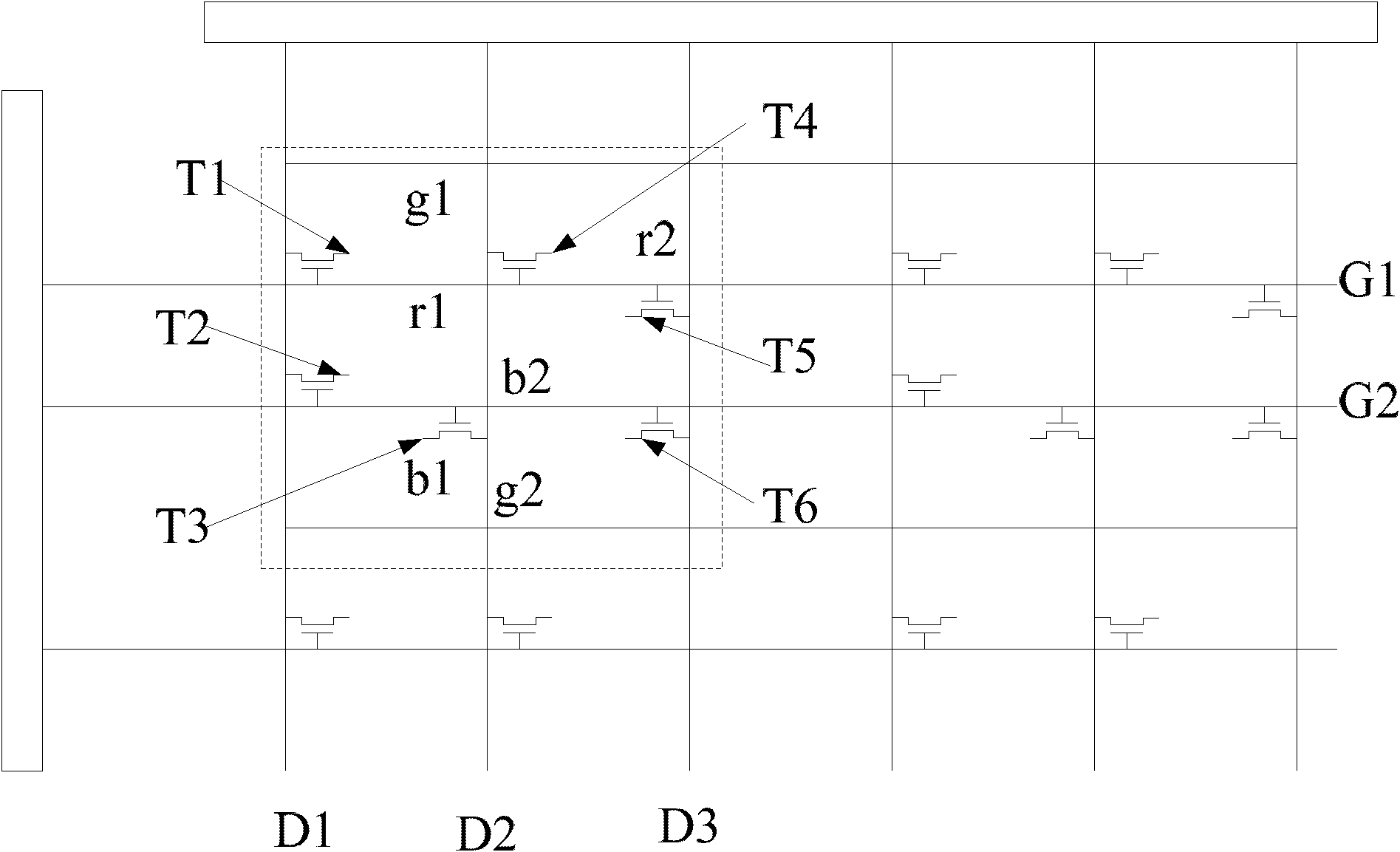
[0046] This embodiment discloses a thin film transistor liquid crystal display array substrate, including:
[0047] Two main pixel regions adjacent along the first direction, wherein each main pixel region respectively includes three sub-pixel regions adjacent along the second direction;
[0048] two gate lines, the two gate lines are arranged on the first metal layer along the first direction;
[0049] two common lines, the two common lines respectively correspond to two main pixel regions, and are arranged on the second metal layer;
[0050] Three data lines, the three data lines are arranged on the second metal layer along the second direction;
[0051] The connecting electrode lines are arranged on the third metal layer and are connected to the two common lines in the first direction.
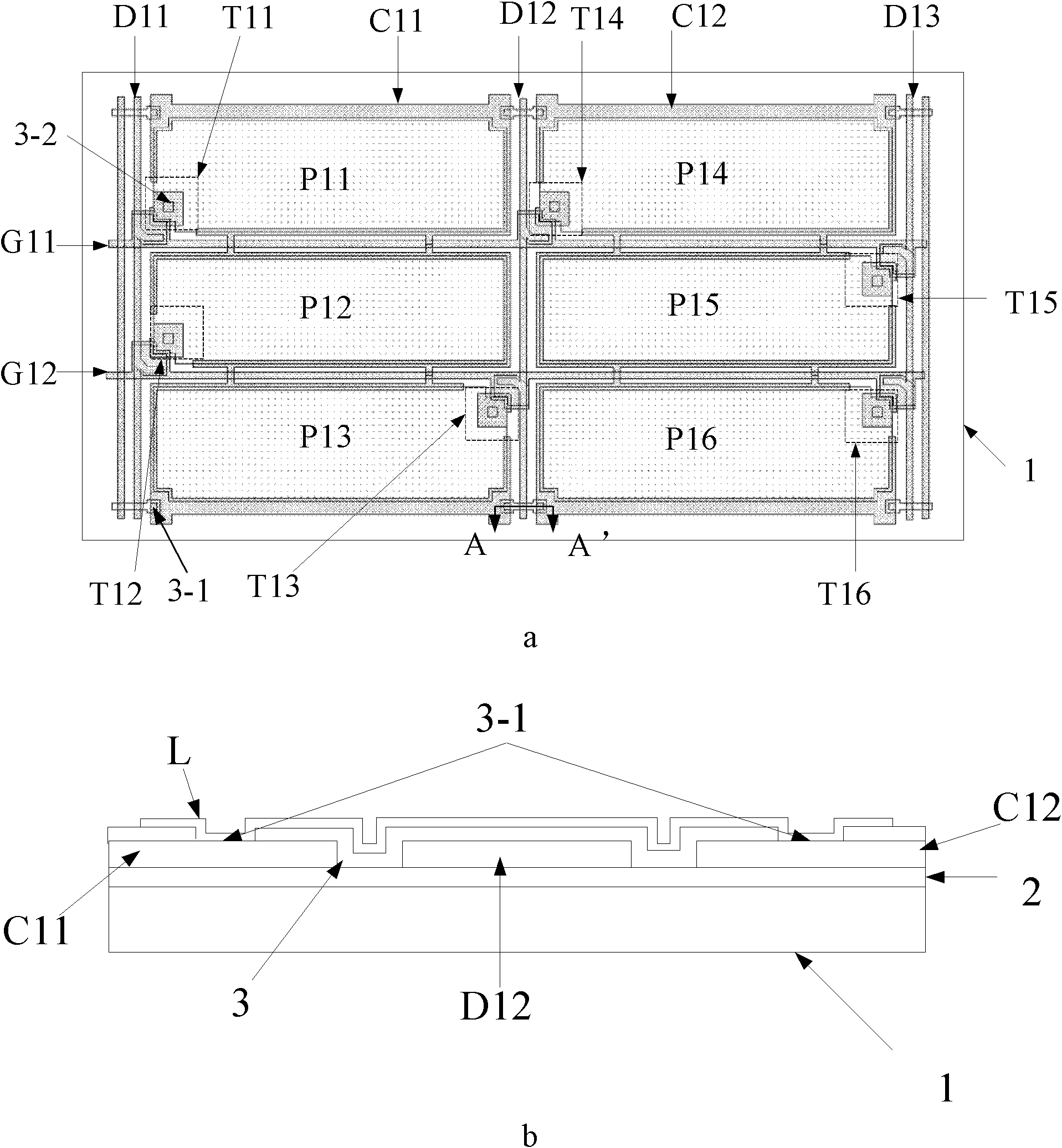
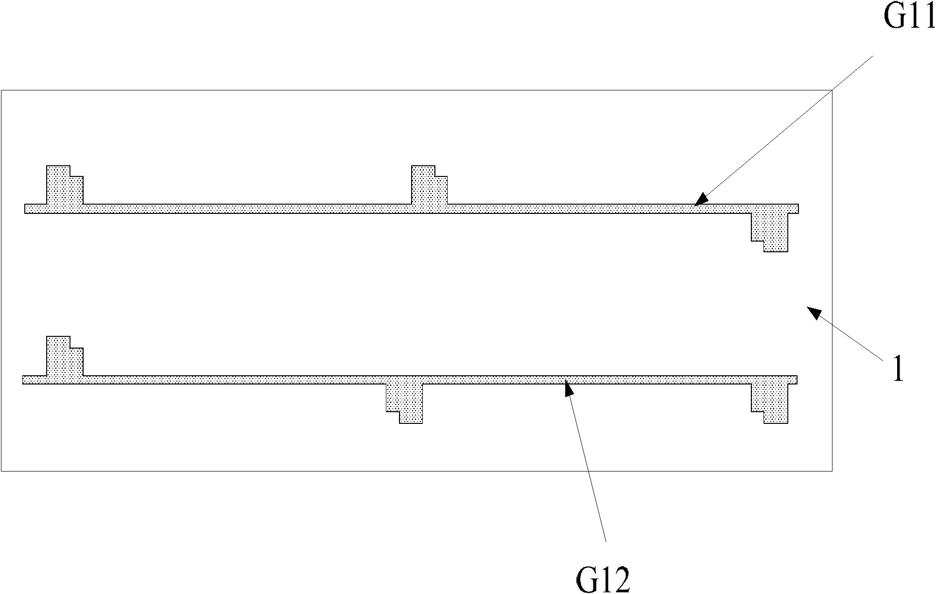
[0052]Specifically, such as figure 2 as shown ( figure 2 -a is the top view, figure 2 -b is a cross-sectional view along the AA' line), the two gate lines G11 and G12 of the thin fi...
Embodiment 2
[0061] This embodiment discloses a manufacturing method corresponding to the thin film transistor liquid crystal display array substrate described in the above embodiments, as Figure 2-Figure 6 As shown, the method includes:
[0062] Step 1: providing a substrate, forming a first metal layer on the surface of the substrate, and etching the first metal layer to form gate lines.
[0063] Specifically, the substrate is a glass substrate or a substrate of other materials.
[0064] Forming the gate lines on the surface of the substrate specifically includes:
[0065] The first metal layer is formed on the surface of the substrate by plasma sputtering, that is, the substrate is first put into the reaction chamber, and the high-energy particles hit the solid flat plate of the target material with high purity, and the atoms are knocked out according to the physical process. The knocked-out atoms pass through the vacuum and finally deposit on the surface of the substrate, resulting ...
PUM
 Abstract
Description
Claims
Application Information
 - R&D
- Intellectual Property
- Life Sciences
- Materials
- Tech Scout
- Unparalleled Data Quality
- Higher Quality Content
- 60% Fewer Hallucinations
Browse by: Latest US Patents, China's latest patents, Technical Efficacy Thesaurus, Application Domain, Technology Topic, Popular Technical Reports.
© 2025 PatSnap. All rights reserved.Legal|Privacy policy|Modern Slavery Act Transparency Statement|Sitemap|About US| Contact US: help@patsnap.com