Mosfet and the method to make the same

A technology of oxide semiconductor and field effect transistor, which is applied in semiconductor/solid-state device manufacturing, semiconductor devices, electrical components, etc., can solve problems such as unfavorable mass production, charge imbalance, etc., to reduce charge imbalance and improve manufacturing capacity , cost-effective effect

Active Publication Date: 2013-06-05
FORCE MOS TECH CO LTD
View PDF4 Cites 22 Cited by
  • Summary
  • Abstract
  • Description
  • Claims
  • Application Information

AI Technical Summary

Problems solved by technology

All these cost increases are not conducive to high-volume production
Moreover, other factors, such as the problem of charge imbalance caused by trapped charges in the columnar structure, remain unresolved.

Method used


Image

  • Mosfet and the method to make the same
  • Mosfet and the method to make the same
  • Mosfet and the method to make the same

Examples


Embodiment Construction

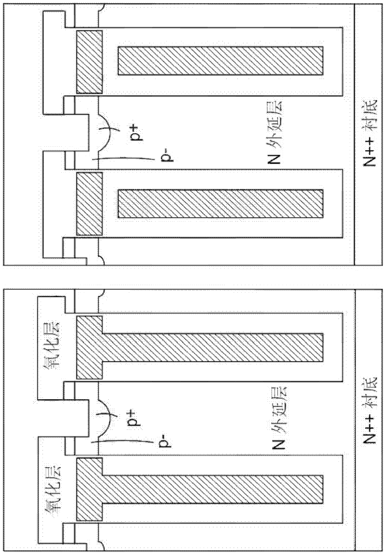
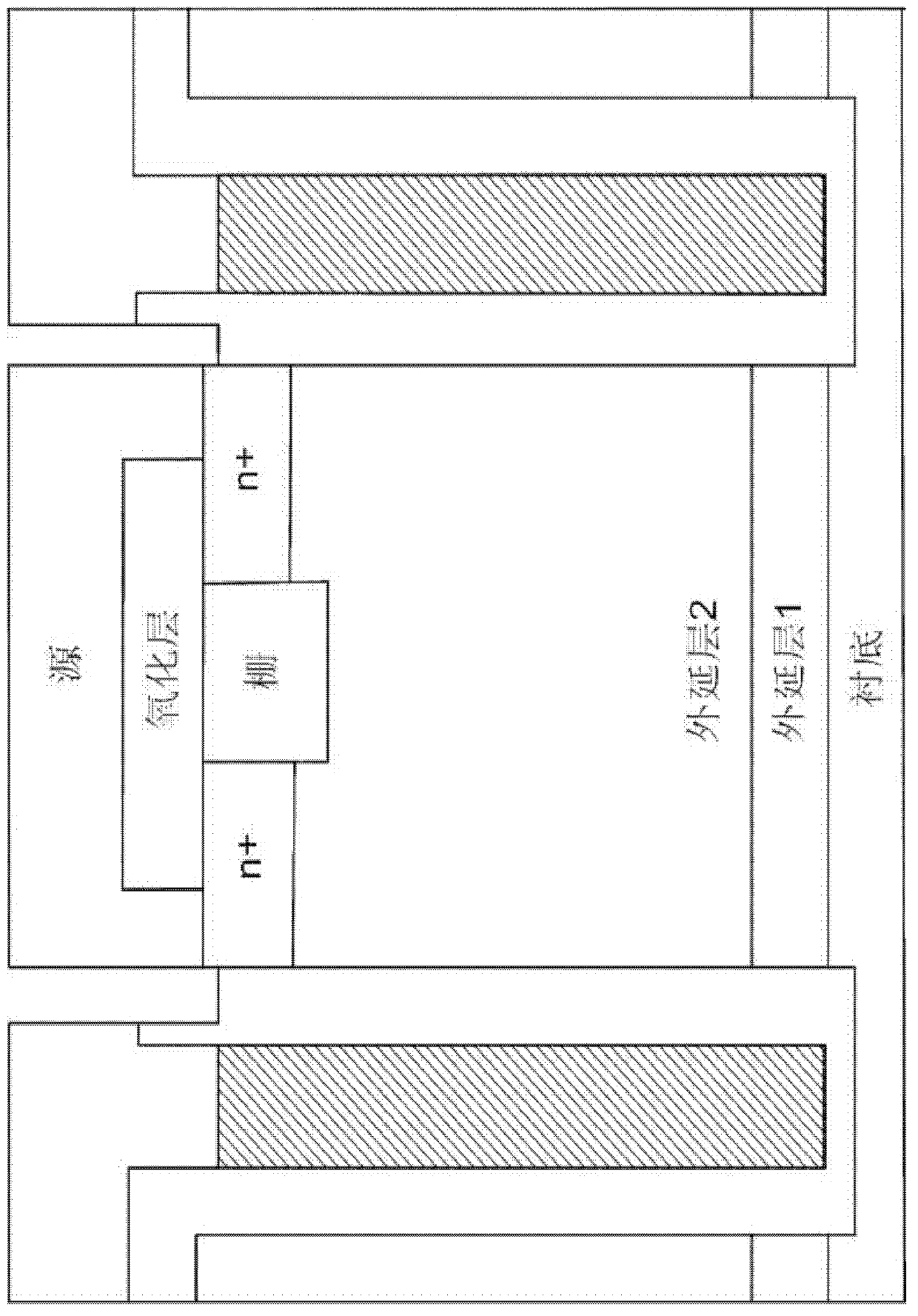
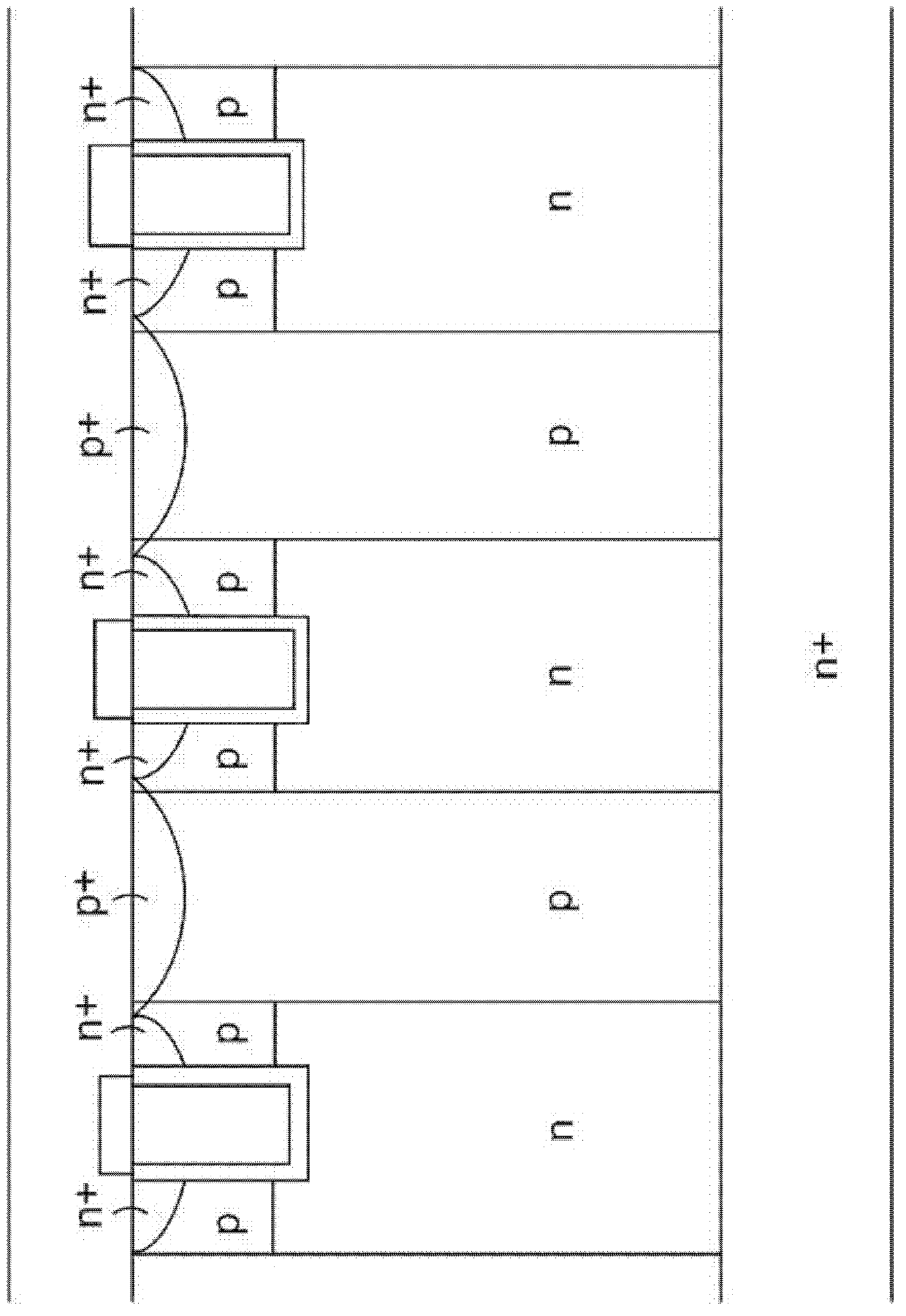
[0038] The invention is explained in more detail below with reference to the accompanying drawings, in which preferred embodiments of the invention are shown. The invention can, however, be embodied in different ways and should not be limited to the embodiments described herein. For example, the description herein refers more to N-channel semiconductor integrated circuits, but clearly other devices are also possible. The following is a detailed description of preferred embodiments for practicing the present invention by referring to the accompanying drawings. Some directional terms, such as "top", "bottom", "front", "rear", "above", "below", etc., are described with reference to the orientation of the various drawings. Since the elements in the embodiments can be placed in many different directions, the orientation terms in the present invention are used for description only and should not be regarded as limitations of the present invention. It should be understood that vari...


PUM


Abstract

The invention discloses a MOSFET of a super-junction trench having a function of reducing surface electric-field stepped oxide and a split grid structure. The inventive structure can apply additional freedom for better optimization and manufacturing capability by tuning thick oxide thickness to minimize influence of charge imbalance, trapped charges, etc. . . . . Furthermore, the fabrication method can be implemented more reliably with lower cost.

Description

[0001] Cross References to Related Applications [0002] This application claims priority to US Patent Application Serial No. 13 / 303,474, filed November 23, 2011, the disclosure of which is incorporated herein by reference in its entirety. technical field [0003] The invention mainly relates to a unit structure, a device structure and a manufacturing process of a power semiconductor device. More specifically, the present invention relates to a new and improved cell structure of a Super-Junction Trench Metal Oxide Semiconductor Field Effect Transistor (Super-Junction MOSFET), a device structure and an improved manufacturing process thereof. Background technique [0004] Compared with conventional trench metal-oxide-semiconductor field-effect transistors (MOSFETs), super-junction trench metal-oxide-semiconductor field-effect transistors are more efficient due to their higher breakdown voltage and lower drain-source resistance. attractive. As we all know, the super junction ...

Claims


Application Information

Patent Timeline
Patent Type & Authority Applications(China)
IPC IPC(8): H01L29/78H01L29/06H01L21/336
Inventor 谢福渊
Owner FORCE MOS TECH CO LTD
Why Eureka
Try Eureka