Thin-film solar cell and manufacture method thereof
A technology of a solar cell and a manufacturing method, applied in the field of solar cells, can solve problems such as unfavorable solar cell efficiency, increased loss, reduced conversion efficiency, etc., and achieves the effects of good light transmittance, improved electrical conductivity, and solving the problem of texturing
- Summary
- Abstract
- Description
- Claims
- Application Information
AI Technical Summary
Problems solved by technology
Method used
Image

Examples
Embodiment 1
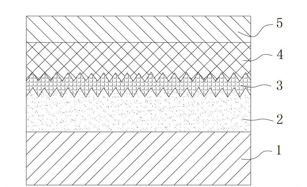
[0094] Such as Figure 1~2 As shown, the thin film solar cell described in this embodiment includes a substrate 1, a compound transparent conductive thin film layer 2 is arranged on one side of the substrate 1, and a silver thin film layer is arranged on the side of the compound transparent conductive thin film layer 2 away from the substrate 1 3. The side of the silver film layer 3 away from the compound transparent conductive film layer 2 is provided with a photoelectric conversion film layer 4 , and the side of the photoelectric conversion film layer 4 away from the silver film layer 3 is provided with a back electrode layer 5 .
[0095] The thickness of the silver thin film layer 3 is 15nm, its optical transmittance is greater than 90%, and its sheet resistance is less than 3Ω / □.
[0096] A suede structure is provided on the side of the compound transparent conductive thin film layer 2 close to the silver thin film layer 3 .
[0097] The method for making the above-mentio...
Embodiment 2
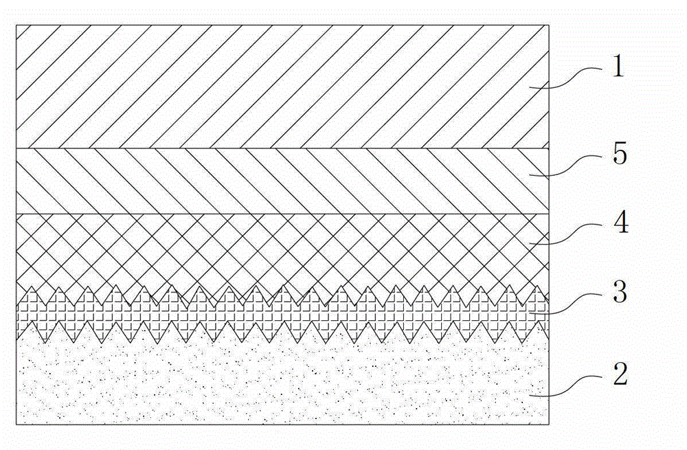
[0109] Such as Figure 3-4 As shown, the thin film solar cell described in this embodiment includes a substrate 1, a back electrode layer 5 is arranged on one side of the substrate 1, and a photoelectric conversion thin film layer 4 is arranged on the side of the back electrode layer 5 away from the substrate 1, and the photoelectric The side of the conversion film layer 4 away from the back electrode layer 5 is provided with a silver film layer 3 , and the side of the silver film layer 3 away from the photoelectric conversion film layer 4 is provided with a compound transparent conductive film layer 2 .
[0110] The thickness of the silver film layer is 15nm, its optical transmittance is greater than 90%, and its sheet resistance is less than 3Ω / □.
[0111] A textured structure is provided on the side of the photoelectric conversion thin film layer 4 close to the silver thin film layer 3 .
[0112] The method for making the above-mentioned thin film solar cell comprises the ...
Embodiment 3
[0124] Such as Figure 5-6 As shown, the thin-film solar cell described in this embodiment includes a substrate 1, a connection layer 6 is arranged on one side of the substrate 1, and a silver thin film layer 3 is arranged on the side of the connection layer 6 away from the substrate 1, and the silver thin film layer 3 A compound transparent conductive film layer 2 is arranged on a side away from the connection layer 6, a photoelectric conversion film layer 4 is arranged on a side of the compound transparent conductive film layer 2 away from the silver film layer 3, and a photoelectric conversion film layer 4 is far away from a side of the compound transparent conductive film layer 2 The back electrode layer 5 is provided on the side.
[0125] The thickness of the silver film layer is 15nm, its optical transmittance is greater than 90%, and its sheet resistance is less than 3Ω / □.
[0126] A textured structure is provided on the side of the compound transparent conductive thin...
PUM
| Property | Measurement | Unit |
|---|---|---|
| Thickness | aaaaa | aaaaa |
| Sheet resistance | aaaaa | aaaaa |
| Sheet resistance | aaaaa | aaaaa |
Abstract
Description
Claims
Application Information
 - R&D
- Intellectual Property
- Life Sciences
- Materials
- Tech Scout
- Unparalleled Data Quality
- Higher Quality Content
- 60% Fewer Hallucinations
Browse by: Latest US Patents, China's latest patents, Technical Efficacy Thesaurus, Application Domain, Technology Topic, Popular Technical Reports.
© 2025 PatSnap. All rights reserved.Legal|Privacy policy|Modern Slavery Act Transparency Statement|Sitemap|About US| Contact US: help@patsnap.com